Low-Cost PCB Manufacturing: PCB Design, PCB Manufacturing & Cost Reduction Guide
PCB design is a broad engineering discipline involving electrical performance, mechanical requirements, manufacturing processes, component selection, thermal management, reliability, and cost control. A PCB may provide excellent electrical performance, but if its manufacturing cost is too high for the target product, it may not be commercially viable.
While some expenses, such as research and development and initial prototyping, are difficult to eliminate, many PCB-related costs can be influenced through careful engineering decisions. Material selection, board dimensions, layer count, stackup structure, copper weight, routing density, manufacturing tolerances, and order volume can all affect the final PCB cost.
The goal of Low-Cost PCB Manufacturing should therefore not be to make the cheapest possible board. Instead, the objective should be to achieve the required electrical and mechanical performance at the lowest practical total cost.
This article explains the main factors that influence PCB cost and discusses how engineers can optimize PCB Design and PCB Manufacturing without compromising essential quality and reliability.
What Determines PCB Quality?
A low-cost PCB is not necessarily a low-quality PCB. Quality should be evaluated against the electrical, mechanical, environmental, and reliability requirements of the intended application.
Several characteristics can provide useful indicators of PCB quality.
Mechanical Strength
Mechanical stability is an important part of PCB quality.
A rigid PCB should maintain its specified shape and dimensional tolerances during normal handling, assembly, and operation. Large or unusually thin boards can be more susceptible to bow and twist.
The appropriate PCB thickness depends on:
- Board dimensions
- Layer count
- Material
- Copper distribution
- Component weight
- Mounting method
- Mechanical loading
- Application requirements
Therefore, reducing board thickness solely to reduce material cost can create mechanical problems if the resulting structure is not suitable for the application.
Signal Integrity
Signal integrity becomes increasingly important as data rates increase.
A properly designed PCB should maintain the required signal quality throughout the transmission path. Excessive attenuation, impedance discontinuities, crosstalk, or poor return paths can cause communication errors or reduced system performance.
For high-speed designs, engineers should consider:
- Controlled impedance
- Trace geometry
- Dielectric thickness
- Reference planes
- Differential-pair routing
- Return-current paths
- Via transitions
- Connector discontinuities
- Material loss characteristics
A cost-optimized PCB should meet the actual requirements of the interface rather than adding unnecessary high-speed features.
Thermal Performance
PCB temperature rise is another important quality consideration.
Excessive heating can result from high current density, insufficient copper cross-section, inadequate thermal paths, poor component placement, or insufficient system-level cooling.
However, it is important to distinguish PCB heating from heat generated by components. A processor, power transistor, LED, or voltage regulator may generate substantial heat even when the PCB itself is appropriately designed.
Copper thickness, trace width, copper area, thermal vias, and ambient conditions all contribute to PCB thermal performance.
A low-cost design should therefore optimize the complete thermal path rather than simply increasing copper thickness everywhere.
Factors That Affect PCB Manufacturing Cost
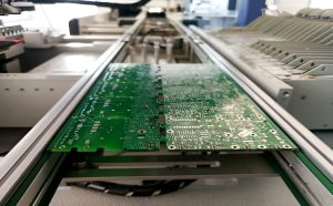
Before attempting to reduce PCB cost, engineers should understand where the cost comes from.
Material Selection
Material is one of the fundamental cost drivers in PCB manufacturing.
FR-4 is widely used because it offers a practical balance of electrical performance, mechanical strength, availability, and cost for many applications.
However, certain applications require specialized materials.
Examples include:
- High-frequency laminates
- Low-loss materials
- High-temperature laminates
- Flexible materials
- Rigid-flex materials
- High-Tg materials
- Thermally conductive materials
Specialized laminates can cost considerably more than standard FR-4 and may require different processing conditions.
The objective should therefore be to select the least expensive material that still satisfies the application’s electrical, thermal, mechanical, and reliability requirements.
PCB Size and Shape
Board size has a direct effect on material utilization and manufacturing economics.
A larger PCB generally consumes more laminate and copper and may reduce the number of usable panels that can be produced from a standard manufacturing panel.
Board shape also matters.
Regular rectangular boards are usually easier to panelize than highly irregular outlines. Complex cutouts, unusual profiles, and excessive routing or milling requirements can increase fabrication time and material waste.
For cost-sensitive PCB Design, designers should consider panel utilization from the beginning.
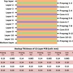
PCB Layer Stackup
The stackup is another major cost factor.
A multilayer PCB requires multiple copper layers, dielectric materials, lamination processes, drilling operations, and inspection steps.
Cost can increase with:
- Higher layer count
- Unusual dielectric thicknesses
- Nonstandard copper weights
- Special laminate materials
- Asymmetric constructions
- Complex sequential lamination
- HDI structures
- Blind and buried vias
A conventional stackup that fits the manufacturer’s standard material portfolio is often easier and less expensive to manufacture than a highly customized structure.
However, reducing layer count should only be done after confirming that the remaining layers can support the required routing, power distribution, signal integrity, and thermal performance.
Advanced PCB Features
Advanced PCB technologies can provide significant electrical and mechanical benefits, but they may also increase manufacturing costs.
Examples include:
- HDI
- Microvias
- Blind vias
- Buried vias
- Via-in-pad
- Fine-pitch routing
- Extremely small drills
- Heavy copper
- Controlled impedance
- Edge plating
- Gold fingers
- Special surface finishes
For example, gold fingers may require selective nickel and hard-gold plating. HDI boards may require sequential lamination and laser-drilled microvias.
These technologies should therefore be used when they solve a real design requirement rather than being added unnecessarily.
Order Quantity and Production Economics
Production volume can significantly influence the unit price of a PCB.
Higher-volume production can distribute tooling, engineering, setup, and manufacturing overhead across more boards.
However, the relationship is not simply that price is always inversely proportional to quantity. Pricing depends on:
- Board specifications
- Production volume
- Panel utilization
- Manufacturing technology
- Material availability
- Setup requirements
- Testing requirements
- Delivery schedule
- Supplier capacity
- Logistics
Prototype, low-volume, and mass-production pricing can therefore differ substantially even when the PCB design is identical.
Lead Time
Expedited manufacturing often requires manufacturers to prioritize a project or use additional production resources.
Standard lead times may allow better production scheduling and material planning, potentially reducing cost.
For this reason, engineers should distinguish between the lowest PCB price and the lowest total project cost.
A slightly higher PCB unit price may sometimes be economically preferable if it avoids production delays, emergency logistics, or redesign costs.
How to Reduce PCB Cost Without Sacrificing Quality
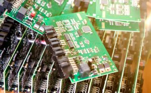
The most effective cost-reduction strategy is to remove unnecessary complexity rather than simply reducing material quantities.
1. Use Advanced Features Only When Necessary
HDI, microvias, strict impedance control, special materials, and other advanced technologies should be applied when required by the electrical or mechanical design.
For example, an ordinary low-speed controller may not need the same stackup or via technology as a high-speed networking board.
Similarly, not every PCB requires:
- Laser-drilled microvias
- Buried vias
- Ultra-fine traces
- Specialized low-loss laminates
- Heavy copper
- Exotic surface finishes
A good PCB Design uses advanced technologies selectively.
2. Optimize the Layer Count
Reducing the number of layers can lower material and fabrication costs, but layer reduction must be performed carefully.
Before removing a layer, engineers should check:
- Routing capacity
- Power distribution
- Ground-plane continuity
- Signal return paths
- Impedance control
- Thermal requirements
- EMI/EMC performance
- Via count
- Manufacturing tolerances
A 6-layer PCB is not automatically more economical than an 8-layer PCB if forcing the design into six layers creates complex routing, additional HDI features, or manufacturing difficulties.
The lowest layer count is therefore not always the lowest total-cost solution.
3. Use DFM During PCB Design
Design for Manufacturing (DFM) is one of the most effective approaches to controlling PCB cost.
DFM reviews whether the design can be manufactured efficiently using the supplier’s standard processes.
Important parameters include:
- Minimum trace width
- Minimum spacing
- Drill diameter
- Aspect ratio
- Annular ring
- Copper thickness
- Board thickness
- Solder mask clearance
- Surface finish
- Panelization
- Edge clearance
Designers should use the manufacturer’s capabilities rather than arbitrary generic values.
For example, if a supplier can reliably manufacture a larger via with a standard process, there may be little reason to specify a smaller, more expensive via.
4. Optimize Copper Distribution
Copper thickness should be selected according to current, thermal, impedance, and mechanical requirements.
Increasing copper thickness across the entire board can increase cost and complicate etching.
Instead, engineers can optimize current-carrying paths using:
- Wider traces
- Copper pours
- Power planes
- Parallel routing where appropriate
- Additional vias
- Local heavy-copper structures when genuinely required
For example, a power network may be designed using broad copper regions and appropriately distributed vias rather than increasing copper weight across every PCB layer.
The exact solution should be validated against current density, temperature rise, voltage drop, and manufacturing capability.
5. Choose Materials Economically
The most expensive laminate is not necessarily the best choice for every PCB.
A practical material-selection process should consider:
- Required electrical performance
- Operating frequency
- Signal-loss requirements
- Thermal requirements
- Mechanical requirements
- Reliability requirements
- Material availability
- Manufacturing compatibility
- Total cost
Standard FR-4 may be sufficient for many digital and industrial applications.
For high-speed or RF designs, specialized materials from suppliers such as Rogers, Isola, and Panasonic may be appropriate.
However, the specific laminate grade should be selected according to the actual design requirements. High-performance material should not be specified simply because it is technically available.
6. Standardize PCB Specifications
Standardization can significantly simplify manufacturing.
Where the application permits, designers can use standard:
- Board thicknesses
- Copper weights
- Dielectric materials
- Drill sizes
- Surface finishes
- Trace/space rules
- PCB dimensions
Using a manufacturer’s standard material and process portfolio can reduce setup complexity and improve production efficiency.
7. Optimize PCB Panelization
Panelization determines how efficiently individual boards are arranged on a manufacturing panel.
Good panel utilization can reduce material waste and improve production economics.
Designers and manufacturers should consider:
- Board dimensions
- Board orientation
- Routing space
- Tooling rails
- Breakaway methods
- V-score compatibility
- Mouse-bite requirements
- Copper balance
A small change in PCB dimensions can sometimes improve panel utilization substantially.
8. Balance Performance and Cost
Cost optimization should always consider the complete product.
For example, reducing PCB cost by using a thinner board may appear attractive initially. However, if the thinner board requires additional mechanical support, special assembly fixtures, or causes reliability problems, the total product cost may increase.
Similarly, using a lower-cost laminate may reduce PCB material cost but increase signal losses or require additional design compensation.
Therefore, the correct objective is not simply:
Lower PCB Price = Better Design
Instead:
Optimized PCB Cost = Required Performance + Manufacturability + Reliability + Appropriate Material and Process Selection
Smart Engineering Strategies for Low-Cost PCB Design
Creative engineering can sometimes reduce cost without reducing performance.
For example, a power distribution network may use appropriately sized copper planes or parallel conductors connected with multiple vias rather than increasing copper thickness across the entire PCB.
Another example is structural integration.
A thin PCB may be acceptable when the final product includes a rigid mechanical enclosure or mounting structure that provides the required support. In that case, the PCB does not necessarily need to provide all of the mechanical rigidity itself.
However, such approaches should be validated through mechanical, thermal, electrical, and reliability testing.
The key principle is to understand which PCB characteristics are actually required by the complete product and avoid paying for performance that the system does not need.
The Role of the PCB Manufacturer in Cost Reduction
PCB cost optimization should not be treated as the responsibility of the designer alone.
An experienced manufacturer can identify opportunities related to:
- Standard material selection
- Panel utilization
- Manufacturing tolerances
- Via technology
- Copper weight
- Surface finish
- Stackup construction
- Production volume
- Testing requirements
- Lead time
A manufacturer may also suggest an alternative stackup or fabrication process that provides equivalent functional performance at lower cost.
This is why early communication between the design team and PCB supplier is valuable.
PCB Manufacturing Cost Optimization Checklist
| Cost Factor | Cost-Reduction Approach | Important Consideration |
|---|---|---|
| Material | Use the lowest-cost suitable laminate | Verify electrical and thermal requirements |
| Layer Count | Remove unnecessary layers | Maintain routing and reference-plane requirements |
| Board Size | Reduce unnecessary area | Check mechanical and component-clearance requirements |
| Board Shape | Use manufacturable outlines | Improve panel utilization |
| Copper Weight | Use only required copper thickness | Verify current and thermal performance |
| Vias | Avoid unnecessarily small or complex vias | Check routing and reliability |
| HDI | Use only where needed | Confirm whether conventional vias are sufficient |
| Surface Finish | Select application-appropriate finish | Consider assembly and reliability |
| Tolerances | Avoid unnecessarily tight tolerances | Confirm supplier capability |
| Panelization | Optimize board arrangement | Reduce material waste |
| Volume | Consolidate production where practical | Consider inventory and demand |
| Lead Time | Use standard production schedules | Balance cost against project timing |
Why Low-Cost PCB Manufacturing Does Not Mean Low Quality
The phrase Low-Cost PCB Manufacturing can sometimes be misunderstood.
Low cost should mean eliminating unnecessary expenses, not eliminating necessary engineering controls.
A properly optimized PCB can use:
- Standard materials
- Appropriate layer count
- Manufacturable trace widths
- Standard drill sizes
- Suitable surface finishes
- Efficient panelization
- Practical tolerances
while still meeting the electrical, mechanical, thermal, and reliability requirements of the application.
The difference is that every specification is selected for a reason.
Kingda PCB Manufacturing Cost Optimization
Kingda supports PCB projects that require a balance between performance, reliability, manufacturability, and cost.
During the quotation and engineering process, factors such as material selection, layer count, copper thickness, PCB dimensions, stackup, via structures, surface finish, impedance requirements, and production volume can be reviewed together.
For customers developing cost-sensitive products, early DFM analysis can help identify unnecessary manufacturing complexity before production begins.
The goal is to create a PCB that satisfies the required product specifications without adding unnecessary material or processing costs.
Conclusion
The key to Low-Cost PCB Manufacturing is not simply choosing the cheapest material or reducing the number of PCB layers. Effective cost optimization requires a systematic evaluation of design requirements, manufacturing processes, materials, tolerances, production volume, and total product economics.
Engineers can reduce PCB costs by using advanced technologies only when necessary, optimizing layer count, selecting appropriate materials, improving panel utilization, standardizing fabrication specifications, and applying DFM principles early in the PCB Design process.
At the same time, essential electrical and mechanical performance should never be sacrificed simply to achieve a lower unit price.
A well-optimized PCB is one that delivers the required signal integrity, thermal performance, mechanical stability, reliability, and manufacturability at an appropriate cost.
By combining careful PCB Design with efficient PCB Manufacturing, manufacturers and engineers can create commercially viable circuit boards that balance performance, quality, and production economics.