High-Frequency PCB: PCB Design, PCB Manufacturing & RF Circuit Board Guide
High-frequency electronics have become an essential part of modern communication, radar, aerospace, automotive, medical, and wireless systems. As operating frequencies move from megahertz (MHz) into gigahertz (GHz) ranges, PCB designers must deal with electrical effects that are often negligible in conventional low-frequency circuits. Transmission-line behavior, dielectric loss, impedance control, signal reflection, crosstalk, and electromagnetic interference (EMI) can all have a significant impact on circuit performance.
For this reason, High-Frequency PCB technology requires a different approach to material selection, stackup planning, routing, fabrication, and testing compared with conventional FR-4 circuit boards.
This guide explains what a high-frequency PCB is, its key characteristics, suitable materials, major manufacturing processes, common manufacturing challenges, and practical PCB Design considerations for RF, microwave, 5G, radar, and other high-speed applications.
What Is a High-Frequency PCB?
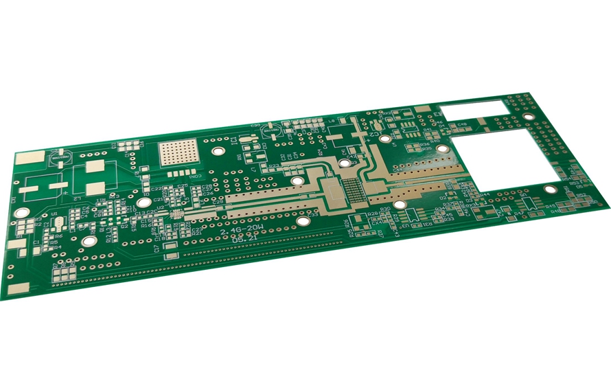
A high-frequency PCB is a printed circuit board designed to operate with signals whose electrical behavior is strongly affected by high-frequency transmission-line effects. Depending on the application, these boards may handle signals ranging from hundreds of megahertz to several gigahertz or higher.
Typical applications include:
- RF communication systems
- 5G wireless equipment
- Microwave circuits
- Radar systems
- Satellite communications
- Aerospace and defense electronics
- Automotive radar
- High-speed networking equipment
- Medical imaging and instrumentation
- Wireless modules and antennas
Unlike a conventional low-frequency PCB, a high-frequency circuit cannot always be treated as a simple collection of lumped components and short interconnections. At sufficiently high frequencies, PCB traces behave as transmission lines. Their geometry and surrounding dielectric environment directly influence impedance, propagation delay, insertion loss, and signal integrity.
Therefore, High-Frequency PCB Manufacturing must closely coordinate material properties, layer stackup, trace geometry, copper characteristics, drilling, lamination, and inspection.
Key Characteristics of High-Frequency PCBs
Signal Transmission and Dielectric Properties
The dielectric constant, commonly represented by Dk or relative permittivity, influences the propagation velocity and impedance of a transmission line. Dielectric loss, commonly represented by Df or dissipation factor, influences signal attenuation.
For high-frequency applications, engineers often select materials with controlled and relatively stable Dk and low Df. However, there is no universal requirement that every high-frequency PCB must use the lowest possible Dk. The appropriate material depends on frequency, stackup geometry, impedance requirements, thermal conditions, mechanical constraints, and cost.
Lower dielectric loss can help reduce attenuation, particularly in longer or higher-frequency transmission paths.
Controlled Impedance
Controlled impedance is one of the most important aspects of PCB Design for RF and high-speed circuits.
Interfaces such as HDMI, USB, LVDS, SATA, PCIe, and DDR may use single-ended or differential transmission lines with defined impedance requirements. Common differential impedance targets include 90 Ω and 100 Ω, while other systems may use different values according to their interface specifications.
The actual impedance is determined by several factors, including:
- Trace width
- Trace thickness
- Dielectric thickness
- Dielectric constant
- Distance to the reference plane
- Copper surface profile
- Differential-pair spacing
- Stackup configuration
The often-used ±10% or tighter impedance tolerance should not be treated as a universal requirement. The target and tolerance must be established from the electrical specification and manufacturing capability.
Low Signal Loss
At high frequencies, conductor loss and dielectric loss become increasingly important. Copper roughness can also influence conductor loss because high-frequency current tends to concentrate near conductor surfaces due to the skin effect.
As a result, high-frequency PCB materials and copper foils may need carefully controlled surface characteristics, especially in low-loss RF and microwave applications.
Thermal Management
High-frequency systems may contain RF power amplifiers, processors, converters, and other heat-generating components. Thermal design must therefore be considered together with electrical design.
Depending on the application, thermal management may involve:
- Large copper areas
- Thermal vias
- Copper planes
- Heat sinks
- Thermal interface materials
- Metal chassis or heat spreaders
- Thermally conductive PCB materials
It is important to distinguish thermal conductivity from CTE. Thermal conductivity is normally expressed in W/m·K and describes how efficiently a material conducts heat. CTE describes dimensional expansion with temperature and is typically expressed in ppm/°C. They are different material properties and should not be confused.
Moisture Resistance
Moisture can influence the dielectric behavior of PCB materials and may affect impedance and signal performance. High-frequency laminates are therefore often selected with moisture resistance and environmental stability in mind.
The actual moisture absorption specification varies significantly between materials, so a universal value such as 2% should not be applied to every high-frequency PCB.
Mechanical and Thermal Stability
High-frequency laminates must also maintain suitable mechanical properties during fabrication and operation. Dimensional stability is particularly important because small changes in dielectric thickness or layer registration can influence controlled impedance.
For demanding applications, engineers may select PTFE-based, ceramic-filled, hydrocarbon/ceramic, or other specialized laminate systems instead of conventional FR-4.
High-Frequency PCB Materials
Material selection is one of the most important decisions in High-Frequency PCB Manufacturing.
FR-4 is widely used throughout the PCB industry and can support many moderately high-speed applications. However, conventional FR-4 may not provide sufficiently low dielectric loss or tightly controlled dielectric properties for demanding RF and microwave designs.
Common high-frequency material families include:
| Material Family | Typical Characteristics | Common Applications |
|---|---|---|
| Rogers high-frequency laminates | Controlled Dk, low Df, RF performance | RF, microwave, radar |
| RT/Duroid series | Low-loss PTFE-based materials | Microwave and RF |
| RO4000 series | Hydrocarbon/ceramic systems with RF characteristics | Wireless, automotive, RF |
| Isola high-speed/high-frequency materials | Controlled electrical and thermal properties | High-speed digital and RF |
| Taconic materials | Low-loss RF laminates | Antennas, microwave, wireless |
| Arlon materials | RF and microwave-oriented laminate options | Aerospace, RF, communications |
Material values such as Dk and Df depend on the specific laminate grade, frequency, test method, resin content, and construction. Therefore, designers should always use the manufacturer’s datasheet and the actual stackup construction rather than relying on generic material values.
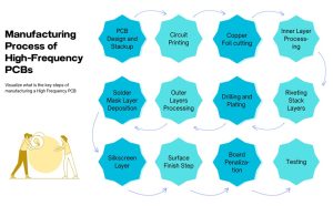
High-Frequency PCB Manufacturing Process
The basic PCB fabrication sequence is similar to conventional multilayer PCB manufacturing, but high-frequency boards generally require tighter control over materials, dimensions, registration, copper geometry, and surface characteristics.
1. PCB Design and Stackup Planning
The manufacturing process begins with a well-defined PCB Design.
Before fabrication, engineers and the PCB manufacturer should review:
- Layer count
- Material selection
- Dk and Df
- Controlled impedance requirements
- Copper thickness
- Trace width and spacing
- Differential-pair geometry
- Via structures
- Reference planes
- RF component placement
- Thermal requirements
- EMI/EMC constraints
The stackup should provide continuous reference planes and controlled dielectric geometry around critical transmission lines.
For high-frequency applications, hybrid stackups combining high-frequency laminate with FR-4 may also be possible when properly engineered. However, the material transition must be considered carefully because differences in Dk, CTE, thermal behavior, and processing requirements can affect performance and manufacturability.
2. Material Preparation
The selected copper-clad laminates, cores, and prepreg materials are prepared according to the approved stackup.
Material thickness, copper weight, dielectric construction, and dimensional tolerances must be controlled because they directly influence impedance and board thickness.
3. Inner-Layer Circuit Formation
The inner copper layers are cleaned and coated with photoresist. The circuit pattern is transferred through exposure and developed before unwanted copper is etched away.
High-frequency designs require particular attention to trace geometry because variations in line width or copper profile can affect controlled impedance and insertion loss.
4. Lamination and Layer Registration
Multilayer structures are assembled using cores and prepreg.
The layers are aligned and laminated under controlled temperature and pressure. High-frequency materials can have processing characteristics that differ from standard FR-4, so the laminate supplier’s recommended processing conditions should be followed.
Registration accuracy is particularly important when narrow dielectric spacing, fine-pitch structures, or high-speed differential pairs are involved.
5. Drilling and Via Formation
Mechanical drilling, laser drilling, or a combination of technologies may be used depending on the design.
Via design is important in high-frequency circuits because unnecessary via stubs can create discontinuities and resonant structures.
For suitable designs, Backdrill PCB technology can remove unused portions of plated through-holes and reduce the electrical effect of long via stubs.
Backdrilling is not automatically required for every high-frequency board. Its use depends on signal rise time, frequency content, via geometry, stackup, and the electrical requirements of the system.
6. Copper Plating
After drilling, the exposed hole walls are prepared and metallized. Electroless copper deposition and subsequent electroplating establish the conductive connection between layers.
Copper thickness and plating uniformity must meet the fabrication specification while maintaining the required trace geometry.
7. Outer-Layer Processing
The outer-layer circuit pattern is formed through imaging, plating, etching, and related processes.
High-frequency transmission lines on the outer layer require consistent geometry. Trace width, copper thickness, solder mask proximity, and the underlying dielectric structure can all influence electrical behavior.
8. Solder Mask Application
Solder mask protects exposed copper from contamination, moisture, and accidental solder bridging.
However, high-frequency designers should consider whether solder mask overlaps critical RF transmission lines. Because solder mask has different dielectric properties from the surrounding air or laminate, it can alter the effective dielectric environment of exposed traces.
For particularly sensitive RF structures, the design may specify solder-mask clearance around certain transmission lines.
9. Silkscreen Application
Reference designators, polarity indicators, part numbers, and other markings are applied during the silkscreen process.
Silkscreen should not overlap solderable pads, RF contact areas, or other functional structures.
10. Surface Finish
The exposed copper is protected using a suitable surface finish.
Common options include:
- ENIG
- HASL
- OSP
- Immersion silver
- Immersion tin
The appropriate finish depends on solderability, flatness, corrosion resistance, assembly process, contact requirements, cost, and electrical considerations.
For high-frequency applications, the surface finish should also be evaluated in relation to critical RF pads, connectors, and conductor geometry rather than selected solely on the basis of general PCB preference.
11. PCB Profiling and Separation
After fabrication and inspection, the individual boards are separated from the production panel using routing, V-scoring, laser processing, or another appropriate method.
Dimensional accuracy is important for RF modules, antennas, edge connectors, and mechanically constrained assemblies.
12. Inspection and Electrical Testing
Quality control may include:
- Automated Optical Inspection (AOI)
- Electrical open/short testing
- Dimensional inspection
- Cross-sectional analysis
- Copper thickness inspection
- Solderability testing where required
- Impedance testing
- TDR measurements
- X-ray inspection for suitable applications
The specific test plan should be determined by the product requirements and applicable manufacturing specifications.
High-Frequency PCB Design Guidelines
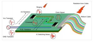
A reliable high-frequency circuit starts with appropriate PCB Design practices.
Keep High-Speed Signals Short
Critical RF and high-speed transmission lines should generally be kept as short as practical to reduce insertion loss and unnecessary discontinuities.
Avoid unnecessary bends, vias, connectors, and layer transitions.
Maintain Continuous Reference Planes
High-frequency transmission lines require a controlled return-current path.
A signal routed over a continuous reference plane generally provides a more predictable return path than a signal crossing plane splits or voids.
Designers should therefore avoid routing critical high-speed signals across gaps in reference planes.
Control Differential-Pair Geometry
Differential pairs should maintain consistent:
- Trace width
- Pair spacing
- Length where matching is required
- Reference-plane relationship
- Via structure
Length matching should be based on the actual timing requirements rather than applied mechanically to every signal.
Minimize Via Discontinuities
Every via introduces a transition between routing layers.
For high-speed and RF signals, designers should evaluate:
- Via pad size
- Antipad dimensions
- Via stub length
- Return vias
- Layer transition geometry
- Local reference-plane structure
Backdrilling or alternative via structures may be used when electrical analysis shows that they provide a meaningful benefit.
Separate RF and Noisy Circuits
Sensitive RF paths should be isolated from noisy switching regulators, high-current power circuits, clocks, and other aggressive signal sources where practical.
However, simply separating circuits by physical distance is not enough. Grounding, return paths, shielding, stackup, filtering, and power integrity must also be considered.
Consider EMI and EMC Early
EMI control should begin during schematic and stackup planning rather than being treated as a final-stage correction.
Useful measures may include:
- Continuous ground planes
- Controlled return paths
- Appropriate layer transitions
- Ground stitching vias
- Shielding structures
- Filtering
- Careful connector placement
- Short current loops
Use Appropriate Copper Roughness
For very high-frequency or low-loss transmission lines, copper surface roughness can contribute to conductor loss.
The appropriate copper foil should therefore be selected according to the frequency range, insertion-loss budget, fabrication capability, and material system.
Common Challenges in High-Frequency PCB Manufacturing
Thermal Management
RF power circuits can generate substantial heat. Excessive temperature can affect component reliability, laminate properties, dimensional stability, and long-term performance.
Thermal design should therefore be integrated into the stackup and component-placement strategy.
Via Stubs and Signal Reflection
A long through-hole via that extends beyond the active signal layer can behave as a capacitive or resonant discontinuity at high frequencies.
Backdrilling can remove unused via sections, but the decision should be based on actual signal requirements.
Copper Thickness and Trace Geometry
Maintaining consistent copper geometry becomes more challenging when a design combines heavy copper, fine lines, tight spacing, and controlled impedance.
Fabrication rules should therefore be reviewed with the PCB manufacturer before production.
Solder Mask Effects
Solder mask changes the dielectric environment around exposed copper. For particularly sensitive RF transmission lines, this can influence impedance and loss.
The designer should specify solder-mask openings where required by the RF design.
Material Compatibility
High-frequency laminates may have different lamination, drilling, thermal expansion, and surface-treatment characteristics from standard FR-4.
When different laminate systems are combined, the manufacturer must validate the complete manufacturing process.
Dimensional and Registration Control
At high frequencies, even relatively small changes in trace width, dielectric thickness, or layer registration can influence impedance.
Therefore, dimensional tolerances should be defined according to the electrical requirements instead of using unnecessarily tight tolerances everywhere.
High-Frequency PCB vs Conventional PCB
| Feature | Conventional PCB | High-Frequency PCB |
|---|---|---|
| Typical materials | FR-4 and related laminates | RF, microwave, low-loss, or specialized laminates |
| Main concern | Basic electrical and mechanical performance | Signal integrity, loss, impedance, EMI/EMC |
| Dielectric control | Moderate | Often much tighter |
| Impedance control | Application dependent | Frequently critical |
| Copper roughness | Usually less critical | Can become important |
| Via design | General-purpose | Stub and discontinuity effects may require analysis |
| Stackup | General multilayer planning | Electrical and RF-driven stackup planning |
| Testing | AOI and electrical testing | May additionally require impedance/TDR and RF-specific validation |
| Cost | Generally lower | Often higher due to materials and process control |
Applications of High-Frequency PCBs
High-frequency PCBs are used across many advanced electronic systems, including:
- 5G base stations and wireless communication equipment
- Automotive radar
- Aerospace electronics
- Satellite communication
- Radar navigation
- RF amplifiers
- Microwave modules
- Antenna systems
- Medical imaging equipment
- High-speed networking
- Industrial wireless equipment
- IoT and connected devices
As operating frequencies increase, the PCB becomes an increasingly important part of the overall electrical system rather than merely a mechanical carrier for components.
How to Choose a High-Frequency PCB Manufacturer
Selecting a suitable manufacturing partner requires more than checking whether a supplier can fabricate multilayer boards.
Engineers and purchasing teams should evaluate:
- Material capability — Can the manufacturer process the required RF laminate reliably?
- Controlled impedance capability — Can the supplier fabricate and verify the required impedance?
- Stackup engineering — Can the manufacturer review the proposed stackup and provide DFM feedback?
- Via technology — Does the supplier support microvias, blind/buried vias, or backdrilling when required?
- Dimensional control — Are trace width, dielectric thickness, registration, and board thickness adequately controlled?
- Testing capability — Can the supplier perform AOI, electrical testing, TDR, cross-section analysis, and other required inspections?
- Production experience — Does the manufacturer have experience with RF, microwave, high-speed, or other technically demanding PCB products?
- Documentation and traceability — Can material and manufacturing records be maintained throughout production?
A qualified supplier should participate in the design-for-manufacturing process rather than simply fabricate files without technical review.
How Kingda Supports High-Frequency PCB Projects
Kingda provides PCB engineering and manufacturing support for demanding circuit-board applications. For high-frequency projects, the manufacturing process can be coordinated around material selection, layer stackup, controlled impedance, via structures, copper requirements, surface finish, and inspection requirements.
Working with the manufacturer during the early PCB Design stage can help identify potential fabrication risks before the design reaches mass production.
This approach is especially valuable when the project involves RF signals, microwave frequencies, high-speed interfaces, controlled impedance, specialized laminates, or strict dimensional requirements.
Conclusion
High-frequency PCB technology is fundamentally different from conventional low-frequency circuit-board design because PCB geometry, dielectric properties, conductor characteristics, and interconnect structures can directly affect signal behavior.
A successful High-Frequency PCB requires careful control of material selection, Dk and Df, stackup architecture, impedance, trace geometry, copper roughness, reference planes, via structures, thermal management, and EMI/EMC considerations.
From the perspective of PCB Design, engineers should establish the electrical requirements early and design transmission lines around controlled impedance and predictable return paths. From the perspective of PCB Manufacturing, the selected supplier must be capable of maintaining the required material, dimensional, registration, plating, and testing controls.
For RF, microwave, 5G, radar, aerospace, automotive, and other high-speed applications, close cooperation between the design team and PCB manufacturer is essential for achieving consistent electrical performance and manufacturing reliability.