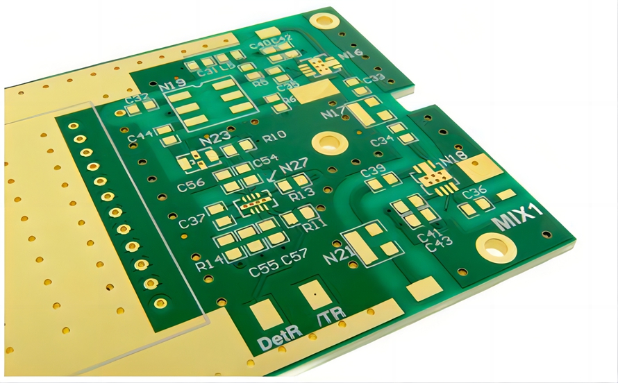
Microwave PCB: RF Materials, PCB Design and PCB Manufacturing Guide
The electronics industry covers a wide range of applications, from wireless communication and radar systems to medical equipment, automotive electronics, and aerospace systems. Despite their differences, these technologies share one fundamental building block: the printed circuit board (PCB).
As electronic systems become faster, smaller, and more sophisticated, conventional PCB technologies may not always provide the electrical performance required by high-frequency applications. This is where Microwave PCB technology becomes particularly important.
Designed to handle RF and microwave signals with controlled electrical characteristics, microwave PCBs are engineered to minimize signal loss, manage impedance, control electromagnetic interference (EMI), and maintain signal integrity at high frequencies. Material selection, stackup design, trace geometry, surface finish, copper characteristics, and manufacturing tolerances all have a direct impact on microwave circuit performance.
This article explains what a microwave PCB is, its key characteristics, commonly used materials, advantages and limitations, major design and manufacturing considerations, material-selection parameters, and typical applications.
What Is a Microwave PCB?
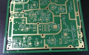
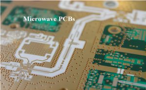
A Microwave PCB is a printed circuit board specifically designed to transmit, control, and process high-frequency signals, particularly RF and microwave signals. Unlike conventional low-frequency PCB designs, microwave circuits are highly sensitive to material properties, transmission-line geometry, parasitic effects, conductor roughness, dielectric loss, and manufacturing tolerances.
Microwave applications commonly operate from the GHz range upward, although the exact definition of RF and microwave frequency ranges varies by industry and application. At these frequencies, even small changes in trace width, dielectric thickness, copper roughness, or dielectric constant can affect impedance and signal integrity.
A microwave PCB therefore requires carefully selected dielectric materials and tightly controlled manufacturing processes. Transmission structures such as microstrip, stripline, and coplanar waveguide (CPW) are frequently used to control impedance and provide predictable signal propagation.
The primary objective is not simply to transmit signals at high speed, but to maintain predictable electrical performance throughout the complete RF signal path.
Key Characteristics of Microwave PCBs
Microwave PCBs have several characteristics that distinguish them from conventional FR-4 circuit boards.
High-Frequency Performance
High-frequency operation is the defining characteristic of a microwave PCB. As signal frequency increases, dielectric loss, conductor loss, dispersion, surface roughness, and parasitic capacitance become increasingly important.
A properly designed microwave PCB uses suitable materials and controlled transmission-line geometries to minimize attenuation and maintain signal integrity.
Controlled Dielectric Properties
The dielectric material has a major influence on signal propagation. Important properties include relative permittivity (Dk), dissipation factor (Df), dielectric thickness, and dielectric uniformity.
Stable dielectric properties help engineers achieve predictable impedance and reduce variations between manufactured boards.
Low Signal Loss
Low-loss materials are essential for many RF and microwave applications. A lower dissipation factor generally reduces dielectric loss, while appropriate copper selection and surface treatment can help control conductor loss.
This becomes increasingly important as operating frequency, transmission distance, and data bandwidth increase.
Controlled Impedance
Impedance Control is one of the most important aspects of microwave PCB Design. Transmission lines must be designed according to their target impedance, which may commonly be 50 Ω in RF systems, although other values are used depending on the circuit architecture.
Trace width, copper thickness, dielectric thickness, Dk, conductor geometry, and reference-plane configuration all affect impedance.
Strong Signal Integrity
Microwave PCBs are designed to maintain signal integrity by controlling:
- Reflection
- Insertion loss
- Crosstalk
- Electromagnetic interference
- Ground discontinuities
- Via parasitics
- Dielectric loss
- Conductor loss
Transmission-line structures such as microstrip, stripline, and coplanar waveguide can be selected according to the requirements of the RF system.
Materials Used in Microwave PCBs
Material selection is one of the most important decisions in microwave PCB development.
Conventional FR-4 can be appropriate for many electronic applications, but high-frequency circuits often require materials with more stable dielectric properties and lower loss characteristics.
Common microwave PCB material families include:
- PTFE-based laminates
- Ceramic-filled PTFE materials
- Hydrocarbon/ceramic laminates
- Low-loss FR-4 and modified epoxy systems
- Ceramic substrates
- Specialized RF/microwave laminates
- Woven-glass-reinforced RF materials
PTFE-Based Materials
PTFE-based laminates are widely used in high-frequency applications because of their low dielectric loss and favorable RF electrical characteristics.
However, PTFE materials can present manufacturing challenges because of their mechanical characteristics and dimensional behavior. Reinforcement and filler systems are therefore used in different formulations to improve mechanical stability and manufacturability.
Ceramic-Filled Materials
Ceramic-filled laminates can provide a useful balance between electrical performance, thermal behavior, dimensional stability, and manufacturing cost.
Depending on the formulation, ceramic fillers can help achieve a more stable dielectric constant and lower thermal expansion than some unfilled polymer systems.
Woven-Glass-Reinforced Materials
Glass reinforcement can improve dimensional stability and mechanical strength. However, the dielectric behavior of woven-glass materials can vary locally because the resin-rich and glass-rich regions have different electrical properties.
This effect can become significant in precision RF applications and should therefore be considered during stackup and transmission-line design.
Advantages of Microwave PCBs
Microwave PCBs provide several important advantages for high-frequency electronic systems.
Higher Bandwidth
Higher operating frequencies can support wider bandwidths, depending on the communication architecture and available spectrum.
This makes microwave PCB technology suitable for applications that require high data throughput, high-resolution sensing, or wideband signal processing.
Reduced Signal Propagation Delay
High-frequency systems can support fast signal transitions and high-speed data processing. However, propagation delay is determined primarily by transmission-line length and the effective dielectric constant rather than frequency alone.
Therefore, PCB designers must optimize both routing geometry and electrical length when designing high-speed RF circuits.
Improved Signal Integrity
Carefully controlled materials, impedance, grounding, and transmission-line structures can reduce unwanted reflections and losses.
This is particularly important in RF front ends, filters, amplifiers, antennas, radar systems, and communication equipment.
Compact Circuit Architecture
Higher-frequency electromagnetic waves have shorter wavelengths, allowing antennas and other RF structures to be made smaller for a given electrical configuration.
This makes microwave PCB technology useful in compact wireless products, portable equipment, automotive radar, and other space-constrained systems.
High-Resolution Sensing
Microwave and RF systems can support precise sensing and measurement. Radar, imaging, satellite communication, and medical equipment can benefit from carefully engineered high-frequency circuits.
Advantages and Limitations of Microwave PCBs
Advantages
The major advantages of microwave PCBs include:
- Low dielectric and conductor losses when appropriate materials and structures are used
- Controlled impedance
- Excellent RF signal integrity
- High-frequency operating capability
- Support for wide bandwidths
- Compact circuit implementation
- Improved control of reflections and electromagnetic interference
- Compatibility with demanding RF and microwave systems
Limitations
Microwave PCB technology also introduces additional challenges.
The materials can be more expensive than standard PCB laminates, particularly for specialized low-loss materials. Manufacturing can also require tighter control of:
- Trace width
- Dielectric thickness
- Layer registration
- Copper thickness
- Surface roughness
- Via geometry
- Lamination conditions
- Etching accuracy
In addition, microwave materials may behave differently during drilling, lamination, plating, and assembly compared with conventional FR-4.
As a result, microwave PCB manufacturing requires close coordination between the circuit designer, material supplier, PCB manufacturer, and assembly team.
Key Microwave PCB Design and Manufacturing Considerations
Successful microwave PCB development requires both careful PCB Design and controlled PCB Manufacturing.
1. Select the Right Base Material
Material selection should be based on the actual electrical, thermal, mechanical, and environmental requirements of the application.
Important parameters include:
- Dk
- Df
- CTE
- Thermal conductivity
- Moisture absorption
- Copper compatibility
- Operating temperature
- Dimensional stability
- Mechanical strength
A material with an attractive Dk value is not automatically the best choice. Engineers must evaluate the complete electrical and mechanical performance of the laminate.
2. Control Impedance
Impedance should be established during the PCB stackup and transmission-line design stage rather than treated as a manufacturing adjustment.
For example, the impedance of a microstrip is affected by:
- Trace width
- Trace thickness
- Dielectric thickness
- Dielectric constant
- Reference-plane distance
- Copper geometry
Manufacturers should receive controlled impedance requirements as part of the fabrication documentation.
3. Optimize Transmission-Line Geometry
Different RF circuits may use different transmission-line structures.
Common structures include:
- Microstrip
- Stripline
- Coplanar waveguide
- Grounded coplanar waveguide
The appropriate structure depends on the required impedance, available board area, layer stackup, grounding strategy, frequency range, and manufacturing capability.
4. Minimize Discontinuities
At microwave frequencies, vias, pads, connectors, bends, layer transitions, and component footprints can behave as electrical discontinuities.
Designers should minimize unnecessary discontinuities and carefully evaluate transitions between transmission-line structures.
Where high-frequency signals change layers, via configuration and return-current paths should be optimized to minimize parasitic inductance and impedance discontinuity.
5. Pay Attention to Grounding
A stable RF ground structure is essential for many microwave circuits.
Ground planes should provide a low-inductance return path, while ground vias can be used strategically around transmission lines, connectors, and sensitive RF sections.
Via fences can also help provide electromagnetic isolation between circuit regions when appropriately designed.
6. Consider Copper Surface Roughness
At high frequencies, current tends to concentrate near the conductor surface due to the skin effect.
As frequency increases, copper surface roughness can contribute to additional conductor loss. Therefore, low-roughness copper may be beneficial for demanding high-frequency applications.
The appropriate copper treatment should be selected according to the operating frequency, loss budget, fabrication process, and reliability requirements.
7. Control Manufacturing Tolerances
Microwave PCB manufacturing is highly sensitive to dimensional variation.
Changes in trace width or dielectric thickness can change the characteristic impedance. Therefore, manufacturers need to maintain appropriate tolerances for:
- Line width
- Line spacing
- Copper thickness
- Dielectric thickness
- Hole diameter
- Registration
- Etching
- Lamination
For demanding designs, impedance testing and other electrical verification methods can be incorporated into the manufacturing process.
Microwave PCB Material Selection: Key Parameters
Choosing the appropriate material requires more than simply selecting a low-Dk laminate.
Dielectric Constant (Dk)
The dielectric constant, more precisely relative permittivity, affects electromagnetic wave propagation and transmission-line impedance.
A stable and predictable Dk is particularly important in precision microwave designs. Designers should also confirm the test method and frequency associated with the manufacturer’s published Dk value because reported values can vary depending on the measurement method.
Dissipation Factor (Df)
Df, also called the loss tangent, indicates dielectric energy loss.
Lower Df materials generally provide lower dielectric loss, making them attractive for applications involving long RF transmission paths, high frequencies, or demanding insertion-loss requirements.
Thermal Conductivity
Thermal conductivity determines how efficiently heat moves through a material.
For high-power RF systems, thermal management becomes increasingly important because amplifiers, power devices, and other components can generate substantial heat.
A microwave laminate with suitable thermal characteristics can help improve system reliability when combined with an appropriate thermal design.
Coefficient of Thermal Expansion (CTE)
CTE describes how much a material expands or contracts as temperature changes.
In multilayer PCBs, differences in CTE between dielectric materials, copper, and other structures can generate mechanical stress during thermal cycling.
The z-axis CTE is particularly important for plated-through-hole reliability, while x-y dimensional stability affects registration and circuit geometry.
Moisture Absorption
Moisture can affect dielectric behavior and electrical performance.
For applications operating in humid environments or requiring highly stable RF characteristics, moisture absorption should be considered during material selection.
Skin Effect and Copper Loss
As frequency increases, AC current becomes increasingly concentrated near the conductor surface. This phenomenon is known as the skin effect.
Consequently, conductor surface characteristics become more important at microwave frequencies. Copper thickness, copper roughness, trace geometry, and plating should therefore be considered as part of the overall loss budget.
Applications of Microwave PCBs
Microwave PCBs are used across many industries where controlled high-frequency performance is required.
Telecommunications
RF and microwave PCBs are widely used in:
- Wireless communication equipment
- Cellular infrastructure
- Satellite communication
- Base stations
- RF modules
- Wireless networking equipment
- Microwave communication systems
These applications require controlled impedance, low loss, and stable RF performance.
Radar and Navigation
Radar systems rely on the transmission and reception of high-frequency electromagnetic signals.
Microwave PCBs can be used in radar front ends, RF transceivers, signal-processing modules, navigation systems, and sensing equipment.
Automotive radar is another important application, particularly as advanced driver-assistance systems increasingly depend on high-frequency sensing.
Medical Electronics
RF and microwave circuits are used in various medical and diagnostic systems.
Applications can include RF components associated with magnetic resonance imaging (MRI), medical imaging, therapeutic equipment, and specialized sensing systems.
These applications typically require stable electrical characteristics and high reliability.
Aerospace and Defense
Aerospace and defense electronics often operate under demanding electrical, thermal, mechanical, and environmental conditions.
Microwave PCBs can be found in:
- Radar
- Satellite systems
- Electronic warfare equipment
- RF communication systems
- Navigation equipment
- Avionics
- High-frequency sensing systems
For these applications, PCB performance must be evaluated together with the requirements of the complete electronic system.
Automotive Electronics
Modern vehicles increasingly incorporate radar, wireless connectivity, positioning, and sensing technologies.
High-frequency PCBs are used in radar modules and other RF systems where signal integrity, thermal performance, compact size, and manufacturing consistency are important.
Microwave PCB Manufacturing Process
The manufacturing process for microwave PCBs must account for the characteristics of RF materials.
A typical production workflow may include:
- Material selection and incoming inspection
- Stackup engineering
- Inner-layer imaging and etching
- Lamination
- Mechanical or laser drilling where appropriate
- Copper plating
- Outer-layer imaging and etching
- Solder mask and surface-finish processing
- Electrical testing
- Dimensional and visual inspection
- RF or impedance verification when required
Not every microwave PCB uses the same process. Material type, layer count, via structure, copper thickness, surface finish, and design density determine the appropriate manufacturing route.
The manufacturer should also understand the material’s lamination behavior and ensure that fabrication parameters are compatible with the selected laminate system.
How to Improve Microwave PCB Design
Engineers can improve microwave PCB performance by applying several design principles:
- Choose RF materials according to the required frequency and loss budget.
- Establish the stackup before finalizing transmission-line dimensions.
- Use controlled-impedance routing for critical RF paths.
- Keep RF transmission paths short where practical.
- Maintain continuous reference planes.
- Minimize unnecessary vias and layer transitions.
- Optimize high-frequency connectors and launch structures.
- Consider copper roughness at higher frequencies.
- Separate sensitive RF sections from noisy digital circuits.
- Provide appropriate RF grounding and shielding.
- Simulate critical structures before manufacturing.
- Work with a PCB manufacturer that understands high-frequency materials and controlled-impedance fabrication.
Microwave PCB vs Conventional PCB
The fundamental difference between a microwave PCB and a conventional PCB is not simply the operating frequency. It is the degree to which electromagnetic behavior becomes a critical part of the circuit design.
| Feature | Conventional PCB | Microwave PCB |
|---|---|---|
| Typical materials | FR-4 and related materials | RF/microwave laminates, PTFE, ceramic-filled materials, specialized low-loss systems |
| Frequency sensitivity | Moderate to high depending on application | Very high |
| Dk/Df control | Important | Critical |
| Impedance control | Required for high-speed designs | Fundamental |
| Copper roughness | Usually less critical | Increasingly important at high frequency |
| Manufacturing tolerance | Application-dependent | Often tighter |
| RF simulation | Sometimes unnecessary | Frequently important |
| Typical applications | Consumer, industrial, general electronics | Radar, RF communication, satellite, microwave, sensing |
The distinction is therefore application-dependent. A high-speed digital PCB can also require many of the same signal-integrity principles used in RF design.
Conclusion
A Microwave PCB is an important technology for modern high-frequency electronic systems. By combining suitable RF materials, controlled transmission-line structures, precise impedance management, reliable grounding, and tightly controlled manufacturing processes, microwave PCBs can support demanding RF and microwave applications.
However, high-frequency performance cannot be achieved through material selection alone. PCB Design and PCB Manufacturing must be considered together. Dielectric properties, copper roughness, stackup geometry, trace dimensions, vias, connectors, thermal behavior, and manufacturing tolerances can all influence the final electrical performance.
For engineers developing radar, telecommunications, aerospace, automotive, medical, or other RF systems, choosing the right microwave PCB material and manufacturing process is an essential part of achieving stable signal integrity, reliability, and product performance.
Article Summary
Microwave PCBs are specialized circuit boards designed for RF and high-frequency applications. Their performance depends on low-loss materials, stable dielectric properties, controlled impedance, appropriate transmission-line structures, effective grounding, and precise manufacturing.
PTFE-based, ceramic-filled, hydrocarbon-based, and other specialized RF laminates can be selected according to frequency, loss requirements, thermal performance, mechanical stability, and cost. During PCB Design, engineers should pay particular attention to Dk, Df, CTE, copper roughness, transmission-line geometry, grounding, and signal transitions.
During PCB Manufacturing, dimensional tolerances, dielectric thickness, copper geometry, layer registration, lamination, and impedance control must be carefully managed. When these factors are properly coordinated, microwave PCBs can provide reliable high-frequency performance for communication, radar, automotive, medical, aerospace, and other advanced electronic applications.