PCB Edge Connectors: Types, Benefits, Applications & PCB Design and Manufacturing
In the electronics industry, reliable electrical connections are fundamental to system performance. Without dependable interconnections, electronic devices cannot function as intended.
A PCB edge connector provides a practical interface for connecting a printed circuit board to another PCB, a backplane, a motherboard, or an external electronic system. By placing conductive contacts along the edge of a circuit board, engineers can create a compact, detachable electrical and mechanical connection without requiring individual wires or soldered connections.
PCB edge connectors are particularly useful when a sub-board needs to be installed, removed, replaced, or serviced repeatedly. They simplify system integration and can make maintenance and rework considerably easier.
For applications requiring high-density interconnection, high data rates, and frequent insertion and removal, proper edge-connector selection and PCB Design are essential for achieving reliable electrical and mechanical performance.
What Is a PCB Edge Connector?
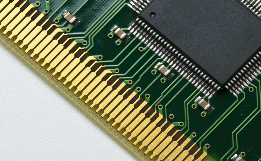
A PCB edge connector is an electrical interface formed by conductive contacts located along the edge of a printed circuit board. The exposed contacts, commonly called edge fingers, are designed to mate with a corresponding connector socket.
Unlike permanent wire-to-board or soldered connections, an edge connector allows the PCB to be inserted into and removed from the mating connector.
A typical edge-connector system consists of:
- PCB edge contacts or edge fingers
- Mating connector housing
- Spring contacts inside the connector
- Mechanical retention features
- PCB edge geometry
- Optional polarization or keying features
The PCB edge contacts are normally plated with a suitable finish to withstand repeated mating cycles and environmental exposure.
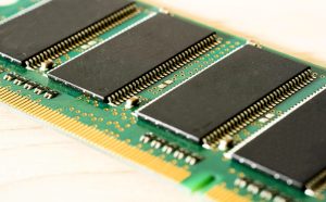
Edge connectors are commonly used for expansion cards, memory modules, communication boards, industrial control boards, and other removable circuit assemblies.
Types of PCB Edge Connectors
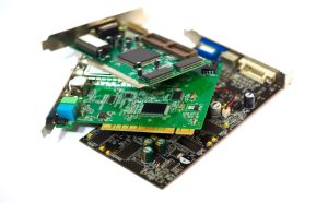
PCB edge connectors can be categorized according to their application and mechanical configuration.
Common applications include:
Embedded System Edge Connectors
Embedded systems often use board-to-board or card-edge interfaces to connect processing, control, communication, and peripheral boards.
These connectors allow individual modules to be replaced without redesigning the entire system.
Display and Control-System Edge Connectors
Display and control equipment may use edge connectors to connect interface boards, display modules, control boards, and other electronic assemblies.
The connector must provide sufficient electrical reliability while meeting the mechanical constraints of the enclosure.
Printer Edge Connectors
Printers and multifunction devices may use card-edge connections for control boards, interface modules, memory, and replaceable electronic assemblies.
PCI Card Edge Connectors
PCI and related expansion-card interfaces are well-known examples of card-edge technology.
A PCB expansion card is inserted into a connector mounted on a motherboard, allowing power, data, and control signals to pass between the two boards.
Modern high-speed expansion interfaces require carefully controlled PCB geometry and connector characteristics to maintain signal integrity.
What Materials Are Used for Edge Connector Contacts?
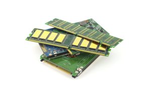
The contact material and surface finish have a major influence on connector durability and electrical reliability.
Common materials and plating systems include:
- Copper alloys
- Nickel
- Gold
- Silver
- Nickel-cobalt alloys
- Other contact materials and underplating systems
Copper alloys are commonly used as the underlying contact material because they provide a useful combination of electrical conductivity, mechanical strength, and manufacturability.
Nickel may be used as an underlayer, while gold plating can provide excellent corrosion resistance and wear resistance.
For PCB edge fingers, hard gold plating is commonly considered when the interface is designed for repeated mating cycles. However, the exact plating system should be selected according to the required insertion cycles, electrical requirements, environmental conditions, and connector manufacturer’s specifications.
Gold provides excellent performance but is more expensive than many alternative finishes, making material selection an important cost consideration.
What Is PCB Edge Beveling?
To make PCB insertion smoother, the edge of a circuit board may be machined with an angled chamfer known as PCB edge beveling.
A bevel creates a gradual leading edge that helps guide the PCB into the mating connector. This is especially useful for card-edge applications involving repeated insertion and removal.
The bevel angle and dimensions should be specified according to the mating connector requirements.
During PCB Manufacturing, the manufacturer must control the board-edge dimensions, plating area, bevel geometry, and mechanical tolerances to ensure compatibility with the connector.
Edge fingers may be plated with suitable contact finishes such as hard gold, depending on the required electrical and mechanical performance.
How Does a PCB Edge Connector Work?
The operating principle of a card-edge connector is relatively straightforward.
1. Insertion
The PCB edge is inserted into the mating connector.
The connector’s spring contacts press against the conductive edge fingers on the PCB.
2. Mechanical Retention
The connector holds the PCB in position using spring contacts, latches, clips, guides, or other mechanical retention mechanisms.
This helps prevent accidental movement or disconnection.
3. Electrical and Signal Transmission
Once the PCB is fully inserted, the connector establishes electrical contact between corresponding conductive paths.
Depending on the application, these connections may carry:
- Digital signals
- Analog signals
- Power
- Ground
- Control signals
- High-speed differential signals
4. Removal and Maintenance
One of the main advantages of card-edge connections is their removability.
The PCB can be removed from the connector for inspection, replacement, troubleshooting, or repair without desoldering individual wires or components.
This makes edge connectors particularly useful for modular electronic systems.
How to Select the Right PCB Edge Connector
Selecting the correct edge connector requires consideration of both electrical and mechanical requirements.
Application Requirements
The application determines the connector’s required:
- Number of contacts
- Contact pitch
- Current rating
- Voltage rating
- Data rate
- Insertion cycles
- Operating temperature
- Mechanical dimensions
High-speed systems may require connectors specifically designed for controlled impedance and low insertion loss.
Electrical Reliability
The connector must maintain stable electrical contact throughout the expected operating life.
Contact resistance, plating quality, contact force, insertion cycles, and environmental conditions can all affect electrical reliability.
For high-speed applications, designers should also evaluate:
- Characteristic impedance
- Insertion loss
- Return loss
- Crosstalk
- Propagation delay
- Differential-pair performance
Compliance Requirements
The selected connector and PCB materials should comply with applicable regulatory and industry requirements.
Depending on the product, these may include:
- RoHS
- REACH
- UL requirements
- IPC requirements
- Product-specific safety standards
Compliance requirements should be confirmed according to the target market and application.
Advantages of PCB Edge Connectors
PCB edge connectors provide several benefits for modular electronic systems.
Easy Sub-Board Installation and Removal
A sub-board can be inserted into or removed from the main board without soldering individual connections.
This makes modular system architecture much more practical.
Easier Maintenance and Repair
If a PCB fails, the entire module can often be removed and replaced without disassembling the entire system.
This can reduce service time and simplify troubleshooting.
Simplified System Integration
Card-edge connectors allow multiple PCB modules to be integrated into a larger electronic system.
A motherboard or backplane can serve as a central interface for multiple removable boards.
Mechanical Support
The mating connector provides mechanical support for the inserted PCB.
Proper connector retention can help reduce movement caused by vibration and mechanical shock. However, the connector alone does not guarantee shock or vibration resistance; the complete mechanical design must be evaluated.
High-Speed and High-Density Interconnection
Modern edge connectors can support high contact densities and high-speed interfaces.
For high-speed applications, the PCB layout and connector must be designed together to maintain signal integrity.
Reduced Wiring
Edge connectors can eliminate many individual cables, wires, and soldered connections.
This can simplify system architecture and reduce assembly complexity.
Convenient Rework
Because the PCB can be disconnected from the main system, technicians can replace or test individual modules more efficiently.
Support for Multiple Signal Types
A single edge connector can carry power, ground, digital signals, analog signals, and communication interfaces.
This makes it suitable for complex modular systems.
PCB Edge Connector Design Considerations
A reliable edge connector depends on more than simply placing copper contacts along the PCB edge.
During PCB Design, engineers should carefully consider several factors.
Edge Finger Geometry
The width, length, pitch, and spacing of the edge fingers must match the mating connector.
Incorrect dimensions can cause poor contact, mechanical interference, or complete incompatibility.
Contact Plating
The plating system should match the expected insertion cycles and environmental conditions.
For frequently inserted cards, wear-resistant contact finishes are especially important.
PCB Thickness
The PCB thickness must fall within the mechanical tolerance of the mating connector.
Even a small mismatch can affect contact force and insertion reliability.
Edge Bevel
The board-edge bevel should be designed according to the connector specification.
The bevel must provide smooth insertion without reducing the effective contact area.
Component Clearance
Components should generally be kept away from the insertion area to prevent mechanical interference with the connector.
This is especially important for components located near the board edge.
Ground and Signal Arrangement
High-speed edge connectors require careful pin assignment.
Ground contacts can be strategically placed between signal groups to reduce crosstalk and provide better return-current paths.
For differential interfaces, the pin arrangement should maintain the required differential-pair geometry as the signals transition through the connector.
Edge Connectors and High-Speed Signal Integrity
As data rates increase, the PCB edge connector becomes part of the overall high-speed transmission channel.
The connector, PCB edge fingers, vias, traces, and mating interface can all contribute to signal degradation.
Important parameters include:
Insertion Loss
Insertion loss represents the reduction in signal power as a signal passes through the interconnection.
Lower insertion loss is generally desirable for high-speed interfaces.
Return Loss
Return loss indicates how much signal energy is reflected due to impedance discontinuities.
Poor impedance matching at the PCB-to-connector transition can increase reflections and degrade signal quality.
Crosstalk
Crosstalk occurs when energy from one signal path couples into a neighboring signal path.
Appropriate contact spacing, ground contacts, connector geometry, and PCB routing can help reduce unwanted coupling.
Controlled Impedance
For high-speed applications, the PCB traces leading to the edge connector should be designed to the required impedance.
The transition from PCB trace to edge finger to connector contact should be considered as one continuous electrical channel.
This is especially important for interfaces operating at high data rates.
PCB Manufacturing Considerations for Edge Connectors
Manufacturing quality directly affects the reliability of card-edge connections.
Important PCB Manufacturing considerations include:
- Edge-finger dimensions
- Plating thickness
- Plating uniformity
- Board thickness
- Edge bevel accuracy
- Copper adhesion
- Board-edge quality
- Dimensional tolerances
- Surface contamination
- Solder mask clearance
The edge-finger plating process should provide a durable contact surface that can withstand the required number of mating cycles.
Manufacturers should also control the board-edge geometry carefully because mechanical tolerances can directly affect connector compatibility.
Common Applications of PCB Edge Connectors
Card-edge technology is widely used across many electronics applications.
Typical examples include:
- Desktop computers
- Graphics cards
- Expansion cards
- Video game consoles
- Medical imaging systems
- Telecommunications equipment
- Industrial control systems
- Data-storage equipment
- Networking equipment
- Embedded computing systems
- Test and measurement equipment
The exact connector design varies significantly according to the electrical performance, mechanical structure, environmental conditions, and service requirements of each application.
Future Trends in PCB Edge Connector Technology
The development of PCB edge connectors is closely linked to the broader evolution of electronic systems.
As products become smaller while data rates continue to increase, connector technology must support higher density and improved electrical performance within increasingly limited space.
Several trends are shaping future edge-connector development.
Higher Data Rates
Modern computing, networking, storage, and communication systems require increasingly high-speed interfaces.
Future edge connectors will need to provide better impedance control, lower insertion loss, reduced crosstalk, and improved signal integrity.
Higher Contact Density
Smaller electronic systems require more electrical connections within limited board space.
This is driving the development of finer-pitch and higher-density connector structures.
Improved Reliability
Applications in automotive, industrial, medical, aerospace, and telecommunications equipment require connectors capable of operating under demanding temperature, vibration, and environmental conditions.
Contact materials, plating systems, mechanical retention, and connector geometry will continue to evolve to address these requirements.
Miniaturization
As electronic devices become smaller, connectors must occupy less PCB area without compromising electrical and mechanical performance.
This creates new challenges for both connector manufacturers and PCB designers.
More Sustainable Materials
Environmental regulations and sustainability goals are encouraging manufacturers to evaluate materials, manufacturing processes, recyclability, and product life cycles.
Future connector development may increasingly emphasize materials and manufacturing methods that reduce environmental impact while maintaining required electrical and mechanical performance.
Conclusion
PCB edge connectors provide a practical and reusable interface between printed circuit boards, backplanes, and electronic systems. Their removable architecture simplifies installation, maintenance, replacement, and system integration.
For high-performance applications, however, edge connectors must be treated as an integral part of the complete PCB Design rather than as an isolated component. Contact geometry, plating, board thickness, edge beveling, impedance, crosstalk, signal routing, and mechanical retention all contribute to the final performance.
During PCB Manufacturing, accurate edge-finger plating, board-edge machining, dimensional control, and connector compatibility are equally important.
As electronic systems continue to demand higher data rates, smaller form factors, greater contact density, and improved reliability, PCB edge connector technology will continue to evolve. By carefully coordinating connector selection, PCB layout, materials, and manufacturing processes, engineers can develop modular electronic systems that are easier to integrate, maintain, and upgrade.
Article Summary
PCB edge connectors provide a detachable electrical and mechanical interface between circuit boards and mating connectors. They are widely used in expansion cards, computers, telecommunications equipment, medical systems, industrial electronics, and other modular applications. Key considerations include edge-finger geometry, contact plating, PCB thickness, beveling, impedance control, crosstalk, insertion loss, and mechanical retention. Successful PCB Design and PCB Manufacturing require close coordination between the PCB layout, connector specifications, materials, plating process, and mechanical requirements. As electronic systems move toward higher data rates, greater density, and smaller form factors, edge connectors will continue to play an important role in modular PCB interconnection.