PCB Assembly Process: Step-by-Step PCBA Guide for PCB Manufacturing
The PCB Assembly Process is one of the most critical stages in the development and production of electronic products. A well-designed PCB cannot function as intended unless its components are correctly placed, soldered, inspected, and tested.
The complete PCBA Process combines material preparation, solder paste printing, component placement, reflow soldering, through-hole assembly, inspection, testing, cleaning, and other processes. Depending on the product requirements, additional steps such as conformal coating, programming, burn-in testing, and functional testing may also be included.
Following a properly controlled PCB Assembly process helps manufacturers reduce defects, improve product reliability, and achieve consistent production quality.
This guide explains the major steps involved in a modern PCB assembly process, from pre-production preparation to final testing and cleaning.
Preparation Before the PCB Assembly Process
Before actual assembly begins, several preparation and verification procedures should be completed. These steps help prevent manufacturing errors and ensure that the required materials, data, and equipment are ready.
DFM Review
Before production starts, the PCB Design documentation should undergo a comprehensive Design for Manufacturability (DFM) review.
The purpose of DFM is to identify design issues that could create manufacturing or assembly problems.
Typical DFM checks include:
- Component footprint accuracy
- Component spacing
- Pad geometry
- Solder mask clearance
- Silkscreen placement
- Via locations
- PCB dimensions
- Assembly orientation
- Thermal considerations
- Manufacturability of fine-pitch components
The BOM, PCB layout, Gerber files, assembly drawings, and other production data should also be reviewed for consistency.
A thorough DFM review can identify potential problems before components are purchased or boards enter production.
Incoming Quality Control (IQC)
Once components arrive at the manufacturing facility, incoming quality control is performed.
The manufacturer checks the received components against the Bill of Materials (BOM), approved part numbers, quantities, specifications, and packaging requirements.
Visual inspection may be used to identify problems such as:
- Deformed components
- Broken leads
- Oxidized terminals
- Damaged packages
- Incorrect part numbers
- Contaminated surfaces
- Improper packaging
For critical, expensive, or highly sensitive components, additional verification may be required.
Depending on the component and customer requirements, testing may involve sampling or full inspection using appropriate test equipment.
Any material that does not meet the approved requirements should be quarantined and investigated before entering production.
Machine Programming and Production Data
After the bare PCB and components are available, the production equipment must be prepared and programmed.
Typical equipment includes:
- Solder paste printers
- Pick-and-place machines
- Reflow ovens
- AOI systems
- SPI systems
- X-ray inspection systems
- THT insertion equipment
- Wave or selective soldering equipment
- ICT equipment
Pick-and-place machines require accurate component-placement data, including component coordinates, rotation, reference designators, and feeder information.
Production data may be generated from PCB CAD and assembly data. Gerber files are primarily used for PCB fabrication, while assembly equipment generally requires dedicated centroid/pick-and-place, BOM, CAD, or machine-specific data.
Accurate production data is essential for maintaining placement accuracy and reducing programming errors.
PCBA Process: Step-by-Step Guide
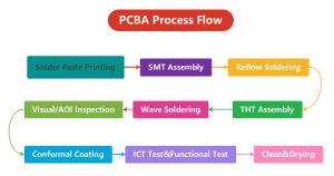
A typical PCBA Process can involve the following steps.
1. Solder Paste Printing
Solder paste printing is normally the first major SMT assembly operation.
A stencil is aligned with the PCB, and solder paste is deposited onto the appropriate component pads.
A squeegee moves across the stencil and forces solder paste through the stencil apertures.
The amount of solder paste deposited depends on factors such as:
- Stencil thickness
- Aperture dimensions
- Solder paste characteristics
- Squeegee pressure
- Printing speed
- PCB surface condition
- Stencil alignment
The stencil must match the PCB pad layout accurately.
For fine-pitch components and small passive components, precise solder paste deposition is particularly important because excessive or insufficient solder can lead to defects.
In many modern assembly lines, Solder Paste Inspection (SPI) is performed after printing to measure paste volume, height, area, and alignment.
2. SMT Component Placement
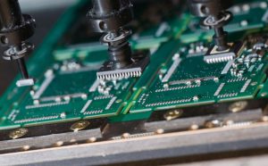
After solder paste printing, surface-mount components are placed on the PCB.
A pick-and-place machine automatically picks components from feeders, trays, or other component packaging and places them at their designated locations.
Modern machines can perform extremely high-speed placement while maintaining precise positional accuracy.
Before placement, the machine may use vision systems to verify component characteristics and orientation.
Important placement parameters include:
- X/Y position
- Component rotation
- Polarity
- Package orientation
- Placement accuracy
- Component spacing
Correct placement is essential because the solder paste and component position must work together during reflow.
3. Reflow Soldering
Once the SMT components have been placed, the PCB passes through a reflow oven.
The board is heated according to a controlled thermal profile. A typical profile includes several stages:
- Preheat
- Thermal soak
- Reflow
- Cooling
During the reflow stage, the solder paste melts and forms solder joints between component terminals and PCB pads.
After cooling, the solder solidifies and creates both mechanical and electrical connections.
The reflow profile must be carefully controlled because excessive temperature or heating time can damage components, while insufficient heating can result in poor solder joints.
Important parameters include:
- Peak temperature
- Time above liquidus
- Heating rate
- Cooling rate
- Thermal uniformity
The correct profile depends on the solder paste, PCB construction, component specifications, and assembly requirements.
4. Post-Reflow Inspection
After reflow soldering, the assembled PCB should be inspected to identify soldering and placement defects.
Automated Optical Inspection (AOI)
AOI uses cameras and image-processing algorithms to inspect the assembled PCB.
It can identify many common defects, including:
- Missing components
- Incorrect components
- Component misalignment
- Polarity errors
- Solder bridges
- Insufficient solder
- Excessive solder
- Open solder joints
AOI provides fast and repeatable inspection for high-volume PCB assembly.
However, AOI cannot directly see every hidden solder joint, particularly those underneath packages such as BGAs.
X-Ray Inspection for BGA Components
X-ray inspection is particularly useful for components with hidden solder connections.
For example, a BGA has solder balls underneath the package, making conventional optical inspection insufficient for examining the entire solder-joint structure.
X-ray inspection can help identify:
- Voids
- Bridging
- Missing solder
- Misalignment
- Abnormal solder-ball structures
- Poor solder connections
The appropriate X-ray inspection method depends on the package, PCB structure, and quality requirements.
5. THT Assembly
Not every component can or should be assembled using SMT.
Through-hole technology (THT), also known as through-hole assembly, is commonly used for components that require mechanical strength, large terminals, or specific electrical characteristics.
During THT assembly, component leads are inserted through the corresponding PCB holes.
Depending on the production volume and component type, insertion may be:
- Manual
- Semi-automatic
- Fully automated
Typical THT components include certain connectors, transformers, switches, large capacitors, and mechanically stressed components.
6. Wave Soldering or Selective Soldering
After through-hole components have been inserted and inspected, the PCB may undergo wave soldering or selective soldering.
Wave Soldering
Wave soldering is an efficient method for soldering suitable through-hole assemblies.
The PCB passes over a controlled wave of molten solder. The solder contacts the exposed component leads and PCB pads, forming solder joints.
Before soldering, the PCB may pass through flux application and preheating stages.
Wave soldering is particularly suitable for boards with a relatively large number of compatible through-hole joints.
Selective Soldering
For mixed-technology boards, selective soldering may be more appropriate.
Selective soldering applies molten solder only to designated through-hole locations rather than exposing the entire underside of the PCB to a solder wave.
This can help protect nearby SMT components and is useful when through-hole and SMT technologies are combined on the same board.
7. Visual Inspection and AOI
After soldering, the PCB assembly undergoes additional inspection.
Visual inspection can identify obvious defects that may not be captured by automated systems.
AOI can also be used to inspect SMT components and solder joints.
Depending on the product, manufacturers may inspect:
- Component placement
- Solder joints
- Polarity
- Lead alignment
- Solder bridges
- PCB contamination
- Mechanical damage
Inspection requirements should be established according to the product’s quality standards and customer specifications.
8. Conformal Coating
Some electronic products require conformal coating to protect the finished PCBA from environmental exposure.
Conformal coating is a thin protective insulating layer applied to the surface of the assembled PCB.
Depending on the coating material, it can provide protection against:
- Moisture
- Dust
- Salt spray
- Chemical contamination
- Corrosive environments
- Condensation
- Certain forms of environmental contamination
Common conformal coating technologies include:
- Acrylic
- Silicone
- Polyurethane
- Epoxy
- Other specialized coating systems
The appropriate coating depends on the operating environment, temperature range, chemical exposure, repair requirements, and reliability expectations.
Before coating, areas such as connectors, switches, test points, and other components that must remain accessible may need to be masked.
Conformal coating should therefore be treated as an application-specific protection process rather than a mandatory step for every PCBA.
9. ICT and Functional Testing
Testing is an important part of the PCB Assembly Process because visual inspection alone cannot verify complete electrical functionality.
In-Circuit Testing (ICT)
ICT uses electrical connections to test individual circuits and components on the assembled PCB.
Depending on the test strategy, ICT may check:
- Continuity
- Resistance
- Capacitance
- Diode characteristics
- Short circuits
- Open circuits
- Component presence
- Certain component values
ICT typically requires a dedicated test fixture and appropriate test software.
Functional Testing
Functional testing evaluates whether the assembled PCB operates according to its intended functional specifications.
For example, a functional test may verify:
- Power consumption
- Communication interfaces
- Input and output signals
- Sensors
- Displays
- Motors or actuators
- Wireless functions
- System-level behavior
For customer-specific products, test procedures, software, fixtures, and acceptance criteria may be supplied by the customer or jointly developed with the assembly manufacturer.
10. Cleaning and Drying
Cleaning requirements depend on the solder paste, flux chemistry, component technology, and product reliability requirements.
If a no-clean process is used and the residues are compatible with the application, extensive post-assembly cleaning may not always be necessary.
For assemblies that require cleaning, flux residues and other contaminants can be removed using an appropriate cleaning process.
Possible cleaning technologies include:
- Aqueous cleaning
- Solvent-based cleaning
- Specialized PCB cleaning systems
- Ultrasonic cleaning for suitable applications
The cleaning method must be compatible with the PCB materials and components.
After cleaning, the PCB assembly should be thoroughly dried before further testing, coating, packaging, or shipment.
Additional PCBA Processes
Depending on the product, customer requirements, and reliability level, the assembly process may include additional operations.
IC Programming
Some PCB assemblies require firmware or software to be programmed into microcontrollers, memory devices, or other programmable components.
Programming can be performed during production testing or as a separate manufacturing operation.
Burn-In Testing
Certain products may require burn-in or extended operating tests.
The purpose is to operate the assembly under controlled conditions for a specified period to identify potential early-life failures.
Thermal Cycling
Products designed for demanding environments may undergo thermal cycling to evaluate their ability to withstand repeated temperature changes.
Final Inspection
Before shipment, the finished PCBA may undergo a final inspection covering:
- Appearance
- Labeling
- Component configuration
- Mechanical dimensions
- Test results
- Coating quality
- Packaging requirements
Common PCB Assembly Defects
Understanding common defects helps manufacturers improve the PCB Assembly Process.
| Defect | Possible Causes | Typical Prevention |
|---|---|---|
| Solder bridge | Excess solder paste, poor stencil design, component spacing | Optimize stencil and printing parameters |
| Insufficient solder | Inadequate paste volume or poor transfer | Optimize stencil apertures and SPI |
| Tombstoning | Uneven wetting or thermal imbalance | Optimize pad geometry and reflow profile |
| Component misalignment | Placement error or solder-paste imbalance | Improve machine setup and inspection |
| Voids | Flux behavior, paste properties, thermal profile | Optimize paste and reflow process |
| Open solder joint | Insufficient solder or poor contact | Improve printing and placement |
| Wrong component | Feeder or BOM error | Barcode and material verification |
| BGA solder defect | Hidden-joint or process issue | X-ray inspection and process control |
PCB Assembly Quality Control
A reliable assembly operation requires quality control throughout the entire production cycle rather than relying only on final inspection.
A typical quality-control system may include:
- DFM review
- BOM verification
- Incoming material inspection
- Solder paste inspection
- Placement verification
- Reflow profile verification
- AOI
- X-ray inspection
- ICT
- Functional testing
- Final visual inspection
- Traceability management
Production traceability can also help manufacturers identify the material batch, machine, operator, test result, and manufacturing conditions associated with a particular PCBA.
How to Improve the PCB Assembly Process
Manufacturers and engineers can improve PCBA quality by focusing on the complete production system.
Optimize the PCB Design
A manufacturing-friendly PCB Design can reduce assembly defects and production costs.
Designers should consider:
- Component spacing
- Pad geometry
- Thermal relief
- Component orientation
- Fiducial placement
- Solder mask clearance
- Test-point accessibility
- Assembly sequence
Improve Stencil Design
Stencil aperture geometry has a direct effect on solder-paste volume.
For fine-pitch components, QFNs, BGAs, and small passive components, stencil design should be optimized for consistent paste transfer.
Control the Reflow Profile
A suitable reflow profile helps ensure consistent solder-joint formation while protecting temperature-sensitive components.
The profile should be verified using appropriate thermal measurement equipment.
Strengthen Material Traceability
Barcode scanning, lot tracking, and component verification can reduce the risk of incorrect material entering production.
Use Multiple Inspection Methods
No single inspection technology can identify every possible defect.
Combining SPI, AOI, X-ray, ICT, functional testing, and visual inspection where appropriate can provide broader process coverage.
Conclusion
The PCB Assembly Process is a carefully controlled sequence that transforms a bare PCB and a collection of electronic components into a functional PCBA.
The process typically begins with DFM review, BOM and material verification, and production-equipment programming. SMT assembly then proceeds through solder paste printing, component placement, and reflow soldering. Depending on the product, THT assembly and wave or selective soldering may follow.
After assembly, AOI, X-ray inspection, ICT, functional testing, cleaning, conformal coating, programming, or other operations may be performed according to the product’s requirements.
A high-quality PCB Assembly process depends on more than advanced equipment. It requires accurate PCB Design, reliable components, optimized process parameters, trained personnel, effective inspection methods, and consistent PCB Manufacturing controls.
By integrating DFM, process control, inspection, testing, and traceability throughout production, manufacturers can improve PCBA consistency and support the reliability requirements of modern electronic products.
Article Summary
The PCB Assembly Process consists of multiple stages, including DFM review, incoming quality control, production-data preparation, solder paste printing, SMT placement, reflow soldering, THT assembly, wave or selective soldering, inspection, testing, cleaning, and optional conformal coating.
Among these steps, solder paste printing, component placement, and reflow soldering are fundamental SMT operations. SPI and AOI can help monitor and inspect the assembly process, while X-ray inspection is particularly valuable for hidden solder joints such as those under BGA packages.
For electrical verification, ICT can test specific circuit characteristics, while functional testing determines whether the assembled PCB performs according to its intended system requirements.
The quality of the final PCBA depends on the interaction between PCB Design, material quality, assembly equipment, process parameters, inspection methods, and PCB Manufacturing controls. A systematic approach to every stage can help reduce defects and improve product reliability.