SMT PCB Assembly Process: 8 Steps for PCB Design and PCB Manufacturing
The electronics industry is developing rapidly, and electronic products are becoming smaller, more powerful, and increasingly complex. To meet these demands, engineers widely use Surface Mount Technology (SMT) and advanced SMT manufacturing processes to achieve high component density, compact layouts, and reliable electrical performance.
When you look inside modern electronic products such as smartphones, computers, medical devices, communication equipment, and automotive electronics, you may wonder how hundreds or even thousands of components are attached to such compact circuit boards. The answer is SMT PCB assembly.
Unlike traditional through-hole assembly, SMT allows electronic components to be mounted directly onto the surface of a printed circuit board (PCB). This approach supports smaller components, higher assembly density, automated production, and efficient high-volume manufacturing.
So, what exactly happens during the PCB SMT assembly process? This article explains the eight major steps involved, from incoming material inspection to final quality assurance.
What Is the SMT PCB Assembly Process?
The SMT PCB assembly process is a manufacturing method in which surface-mount devices (SMDs) are placed directly onto the solder pads on a PCB and then soldered in place.
This differs from through-hole PCB assembly, also known as PTH assembly. In a through-hole process, component leads are inserted through drilled holes in the PCB and soldered to pads on the opposite side or within the plated-hole structure.
SMT assembly offers several important advantages:
- Higher component density
- Smaller PCB and product size
- Better suitability for automated assembly
- Faster production cycles
- Reduced component lead length
- Improved suitability for high-frequency and high-speed applications
- Efficient mass production
For modern electronics, SMT has become a fundamental part of PCB manufacturing and PCBA production.
8 Steps of the SMT PCB Assembly Process
A reliable SMT production line requires much more than simply placing components onto a circuit board. Material verification, solder-paste printing, component placement, reflow soldering, automated inspection, and quality assurance must all work together.
The following eight steps provide a typical overview of the SMT assembly process.
1. Incoming Material Inspection
Incoming inspection is the first step in the SMT PCB assembly process.
Before production begins, manufacturers inspect incoming materials, including bare PCBs, electronic components, solder paste, and other assembly materials. Component information should be checked against the customer’s bill of materials (BOM), approved component list, and engineering documentation.
Important inspection items include:
- Component part number and manufacturer
- Package type and dimensions
- Component quantity
- PCB revision and specifications
- Component polarity and orientation
- Packaging condition
- Moisture-sensitive component requirements
- PCB surface condition
- Solderability and storage conditions
The bare PCB should also be inspected for visible defects such as oxidation, contamination, warpage, scratches, damaged pads, or other conditions that could affect assembly.
For moisture-sensitive devices, appropriate storage and handling procedures are particularly important because absorbed moisture can contribute to package damage during reflow.
Effective incoming inspection helps prevent incorrect components and defective PCBs from entering the SMT production line.
2. Preparation Before SMT Assembly
Once incoming materials have passed inspection, the production team prepares everything required for the specific SMT PCB manufacturing project.
Typical preparation activities include:
- Reviewing PCB design and manufacturing data
- Confirming the BOM and component specifications
- Preparing the solder stencil
- Preparing solder paste
- Loading feeders and component reels
- Preparing pick-and-place machine programs
- Verifying PCB orientation and fiducial marks
- Preparing inspection programs
- Checking moisture-sensitive components
- Baking components when required by the applicable handling requirements
For BGA and other moisture-sensitive packages, baking should only be performed according to the component manufacturer’s specifications and applicable industry requirements.
The solder stencil must also correspond to the PCB pad design. Since different PCB designs have different pad patterns, the stencil aperture layout must be specifically designed for each assembly.
Proper preparation is essential for reducing setup errors and maintaining consistent production quality.
3. Apply Solder Paste
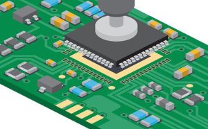
Solder-paste printing is one of the most important steps in the SMT assembly process because the quality of the printed solder paste directly affects the quality of the final solder joints.
A stainless-steel SMT stencil is positioned over the PCB. Solder paste is then deposited through precisely designed stencil apertures onto the PCB pads.
Most modern SMT stencils are manufactured using laser-cutting or other precision fabrication techniques. The aperture dimensions and shapes are optimized according to the component package, pad geometry, solder-paste requirements, and assembly process.
After printing, the PCB should be inspected to verify:
- Solder-paste position
- Paste volume
- Paste height
- Paste coverage
- Pad-to-pad consistency
- Bridging or smearing
- Missing or insufficient solder paste
Solder Paste Inspection (SPI) equipment can be used to automatically measure printed solder-paste deposits and identify printing defects before component placement.
Solder paste should also be stored and handled according to the manufacturer’s specified temperature, shelf-life, thawing, and mixing requirements. The exact storage temperature should not be assumed to be the same for every solder-paste product.
4. Place Components Using a Pick-and-Place Machine
After solder paste has been printed and inspected, the PCB moves to the component placement stage.
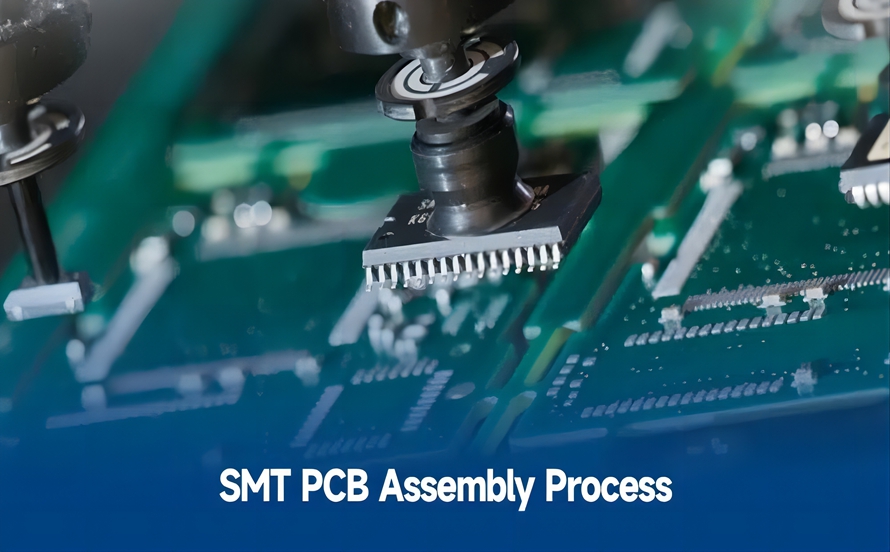
High-speed, high-precision pick-and-place machines automatically pick SMD components from reels, trays, or other feeders and place them at their programmed locations on the PCB.
The machine uses placement coordinates generated from the PCB design and assembly data to accurately position components on their corresponding solder pads.
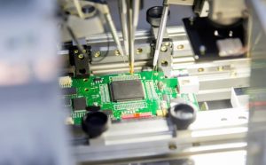
Modern placement systems use machine vision to identify component orientation, package characteristics, PCB fiducials, and placement positions. This helps improve placement accuracy and reduce assembly errors.
Components commonly assembled using SMT include:
- Resistors
- Capacitors
- Diodes
- Transistors
- ICs
- QFNs
- QFPs
- BGAs
- Connectors
- Sensors
- Other surface-mount devices
Before mass production, a first-article or first-board inspection is often performed. Engineers verify component reference designators, values, polarity, orientation, and placement positions before releasing the line for full production.
This step is particularly important for complex PCB Design, where hundreds or thousands of component locations may need to be verified.
5. Solder Components to the PCB
After component placement, the PCB enters the soldering stage.
Reflow soldering is the most widely used soldering method for conventional SMT assembly. During reflow, the PCB passes through a controlled heating profile consisting of multiple thermal zones.
A typical reflow profile includes:
- Preheating
- Thermal soaking
- Reflow
- Cooling
The temperature profile must be carefully controlled according to the solder paste, PCB construction, component requirements, and assembly specifications.
As the PCB moves through the reflow oven, the solder paste melts and forms solder joints between the component terminals and PCB pads. During cooling, the solder solidifies and mechanically and electrically connects the components to the board.
Nitrogen can be used during reflow when required by the process to reduce oxidation and improve soldering performance. However, nitrogen is not universally required for every SMT assembly application.
Vapor-phase reflow is another soldering technology that uses a phase-change medium to transfer heat efficiently. It can be useful for certain prototype, laboratory, or specialized production applications.
For high-volume SMT production, however, convection reflow remains a common approach because it provides programmable thermal profiles and efficient throughput.
The reflow profile should be validated using a thermal profiler rather than relying on a fixed temperature setting. Different PCB designs, component densities, solder alloys, and thermal masses may require different profiles.
6. 100% AOI Inspection
After reflow soldering, automated optical inspection (AOI) is commonly used to identify assembly defects.
AOI equipment uses cameras and image-processing algorithms to inspect the assembled PCB. Depending on the system and inspection strategy, AOI can detect problems such as:
- Missing components
- Incorrect components
- Component misalignment
- Incorrect polarity
- Solder bridges
- Insufficient solder
- Excessive solder
- Open solder joints
- Tombstoning
- Other visible assembly defects
The AOI system compares the actual board against programmed inspection criteria derived from engineering data or a verified reference.
Defective boards can then be separated for engineering review and rework.
AOI provides an important automated quality-control layer, but it does not replace every other form of inspection. Some defects, particularly hidden solder-joint defects beneath BGA packages, may require X-ray inspection.
For high-reliability applications, manufacturers may combine AOI with SPI, X-ray inspection, electrical testing, and functional testing.
7. 100% Visual Inspection
Although AOI provides extensive automated inspection capabilities, visual inspection remains useful in PCB assembly.
Trained inspectors can identify certain conditions that may be difficult for automated systems to classify, including cosmetic PCB defects, contamination, mechanical damage, connector conditions, component markings, and other abnormalities.
Depending on the product and quality requirements, visual inspection may be performed at multiple points throughout the production process.
Typical inspection items include:
- PCB surface condition
- Component placement
- Component orientation
- Solder-joint appearance
- Connector condition
- Mechanical damage
- Contamination
- Scratches or other visible defects
For critical electronic products, combining automated inspection with trained visual inspection provides additional process control.
8. Final Quality Assurance Inspection
After SMT assembly and inspection are completed, the finished PCBA undergoes final quality assurance.
Quality personnel verify the assembled PCB against applicable customer documentation, engineering drawings, BOM requirements, assembly specifications, and inspection criteria.
Depending on the product, final quality assurance may include:
- Visual inspection
- AOI review
- X-ray inspection
- Electrical testing
- ICT
- Functional testing
- Dimensional inspection
- Cosmetic inspection
- Sample-based verification
- Documentation review
For products with strict reliability requirements, additional testing such as burn-in, environmental testing, or other qualification tests may also be performed.
The purpose of final inspection is to verify that the assembled PCB meets the defined technical, electrical, mechanical, and cosmetic requirements before it moves to the next manufacturing stage.
Common SMT PCB Assembly Defects
Even with highly automated production equipment, SMT assembly can experience defects if PCB design, materials, process parameters, or equipment settings are not properly controlled.
| Defect | Possible Causes |
|---|---|
| Solder bridge | Excess solder paste, insufficient pad spacing, poor stencil design |
| Tombstoning | Uneven wetting, thermal imbalance, pad or paste-volume differences |
| Missing component | Placement-machine error, feeder problem, component supply issue |
| Component misalignment | Incorrect placement coordinates, machine setup, PCB fiducial issues |
| Insufficient solder | Incorrect stencil aperture, insufficient paste volume, printing problems |
| Excessive solder | Oversized stencil aperture or excessive paste deposition |
| Voids | Flux behavior, thermal profile, PCB/component structure |
| Open solder joint | Poor wetting, insufficient solder, pad contamination |
| BGA solder defect | Printing, placement, reflow, or hidden-joint process issues |
Understanding these failure modes allows engineers to improve both PCB Design and the manufacturing process.
How PCB Design Affects SMT Assembly
SMT production quality begins long before the PCB reaches the assembly line.
A well-designed PCB should consider manufacturing requirements from the beginning. This approach is commonly referred to as Design for Manufacturability (DFM).
Important considerations include:
Component Footprints
Component footprints must accurately match the manufacturer’s recommended land patterns and assembly requirements.
Incorrect pad dimensions can lead to solder bridges, insufficient solder, tombstoning, or poor solder-joint reliability.
Component Placement
Components should be positioned with sufficient spacing for placement, inspection, rework, and thermal considerations.
High-density layouts should also consider component height, keepout areas, polarity, connector accessibility, and mechanical constraints.
Stencil Design
Stencil aperture design has a direct influence on solder-paste volume.
Fine-pitch components, QFNs, BGAs, and other advanced packages may require customized aperture reductions, shapes, or step stencils to achieve consistent solder deposition.
Thermal Management
Large copper areas, thermal vias, and high-mass components can absorb heat differently during reflow.
The PCB layout and component distribution should therefore be considered when developing the reflow profile.
Fiducial Marks
Fiducial marks provide optical reference points for automated placement and inspection equipment.
Appropriate fiducial design can improve machine alignment and placement accuracy.
SMT vs. Through-Hole PCB Assembly
SMT and through-hole technology are both important assembly methods, but they are suited to different component and product requirements.
| Feature | SMT Assembly | Through-Hole Assembly |
|---|---|---|
| Component mounting | Surface-mounted | Leads inserted through holes |
| Component size | Generally smaller | Often larger |
| Component density | High | Lower |
| Automation | Highly suitable | Suitable, but process-dependent |
| PCB space | Efficient | Requires drilled component holes |
| Mechanical strength | Application-dependent | Often advantageous for mechanically stressed components |
| Typical applications | Consumer electronics, communications, computing, automotive electronics | Power electronics, connectors, industrial equipment, mechanically stressed components |
Many modern products use a combination of SMT and through-hole technologies. This is known as mixed-technology PCB assembly.
How to Improve SMT PCB Assembly Quality
Improving SMT quality requires coordination between design engineering, PCB fabrication, component sourcing, assembly, and testing.
Several practices can significantly improve manufacturing consistency:
- Apply DFM principles during PCB Design.
- Verify the BOM and component specifications before production.
- Use accurate PCB footprints and land patterns.
- Optimize stencil aperture design.
- Control solder-paste storage and handling.
- Perform SPI when appropriate.
- Validate pick-and-place programming before mass production.
- Develop a product-specific reflow profile.
- Use AOI to detect visible assembly defects.
- Use X-ray inspection for applications requiring hidden-joint verification.
- Perform ICT or functional testing when required.
- Track production defects and continuously improve the process.
A strong SMT process is not based on one machine or one inspection method. It depends on the interaction between PCB design, material quality, process control, equipment capability, and inspection.
Applications of SMT PCB Assembly
Because SMT supports compact layouts and automated production, it is widely used across modern electronics.
Common applications include:
- Smartphones and consumer electronics
- Computers and networking equipment
- Automotive electronics
- Medical electronics
- Industrial control systems
- Telecommunications equipment
- IoT devices
- Aerospace and defense electronics
- Power management systems
- LED and lighting products
- Wearable electronics
As electronic products continue to become smaller and more functionally integrated, the importance of reliable SMT PCB assembly will continue to grow.
Conclusion
The SMT PCB assembly process is a highly controlled manufacturing workflow that transforms a bare PCB and electronic components into a functional PCBA. The process typically includes incoming inspection, production preparation, solder-paste printing, component placement, reflow soldering, AOI, visual inspection, and final quality assurance.
The quality of the final assembly depends not only on SMT equipment but also on the PCB layout, component selection, stencil design, solder-paste management, reflow profile, inspection strategy, and manufacturing controls.
For engineers and purchasing teams, understanding the complete SMT process can help identify potential manufacturing risks earlier, improve PCB Design, and achieve more reliable and cost-effective PCB Manufacturing.
Article Summary
SMT PCB assembly mounts surface-mount components directly onto PCB pads and uses automated placement and soldering technologies to produce compact and reliable electronic assemblies. The typical process consists of eight major steps: incoming inspection, pre-production preparation, solder-paste printing, component placement, reflow soldering, AOI inspection, visual inspection, and final quality assurance.
Effective SMT production requires close cooperation between PCB design engineers and manufacturing teams. By applying DFM principles, controlling solder-paste printing, optimizing component placement, validating reflow profiles, and implementing appropriate inspection and testing methods, manufacturers can improve PCBA quality, consistency, and production efficiency.