PCB Reverse Engineering: PCB Design, PCB Manufacturing & PCB Copying Guide
When the original design files of a printed circuit board are unavailable, incomplete, outdated, or lost, reproducing the PCB can become a major challenge. In such cases, PCB Reverse Engineering provides a systematic method for analyzing an existing circuit board and rebuilding its electrical and physical design.
PCB reverse engineering, sometimes referred to as PCB copying or PCB replication, involves examining an existing PCB, identifying its components and connections, reconstructing the schematic and layout, and generating manufacturing data for a new board.
This process can be particularly useful for legacy products, discontinued electronic systems, maintenance projects, obsolete equipment, product redesigns, and replacement PCB production.
However, PCB reverse engineering is more than simply taking a photograph of a circuit board and copying its appearance. A professional process may involve component identification, dimensional measurement, layer analysis, net tracing, electrical testing, schematic reconstruction, PCB Design, and manufacturing verification.
What Is PCB Reverse Engineering?
PCB Reverse Engineering is the process of analyzing an existing printed circuit board to reconstruct its electrical design, physical structure, component information, and manufacturing specifications.
The objective may be to create a functionally equivalent replacement PCB, reproduce an obsolete board, modify an existing design, or recover design information that is no longer available.
Depending on the complexity of the board, reverse engineering may involve analyzing:
- PCB dimensions
- Layer count
- Component locations
- Component part numbers
- Copper traces
- Power and ground structures
- Via locations
- Through-holes
- Blind and buried vias
- Trace widths and spacing
- PCB thickness
- Copper thickness
- Surface finish
- Solder mask
- Silkscreen
- Electrical connections
- Impedance requirements
- Material specifications
For simple single-sided or double-sided PCBs, reverse engineering may be relatively straightforward. Multilayer, HDI, high-speed, RF, or densely populated boards require significantly more advanced analysis.
When Do You Need PCB Reverse Engineering?
If all required manufacturing and assembly files are available and accurate, PCB reverse engineering may not be necessary.
However, reverse engineering can become useful when important design information is unavailable.
Common situations include:
Original PCB Files Have Been Lost
A company may still have functional products in the field even though the original PCB design files are no longer accessible.
Without the original schematic, PCB layout, Gerber files, BOM, and manufacturing drawings, producing an identical replacement can be difficult.
Legacy PCB Designs Need to Be Reproduced
Some electronic products remain in service for many years. Their original PCB may have been designed using obsolete software or manufacturing technologies.
Reverse engineering can help recreate the necessary production data for continued manufacturing or maintenance.
The Original PCB Manufacturer Is No Longer Available
If the original supplier has discontinued production or cannot provide the original design files, analyzing an existing PCB can provide a path toward replacement production.
Replacement Parts Are Required
Industrial equipment, medical systems, automation equipment, and other long-life products may require replacement PCBs long after the original production run has ended.
Existing PCB Designs Need Modification
Reverse engineering can also be used as the starting point for redesigning an existing circuit.
For example, engineers may need to:
- Replace obsolete components
- Improve thermal performance
- Modify connectors
- Change the PCB dimensions
- Improve EMC performance
- Upgrade components
- Reduce manufacturing cost
- Adapt the board to a new enclosure
Files Required for PCB Manufacturing
If the complete PCB manufacturing package is available, reverse engineering may not be required.
The exact documentation depends on the manufacturer and project, but a typical PCB manufacturing and assembly package may include the following files.
1. Schematic
The schematic represents the electrical relationships between components and circuits.
It provides critical information about:
- Component connections
- Power networks
- Ground networks
- Signal paths
- Component values
- Circuit functions
A complete schematic is one of the most valuable files for PCB design verification.
2. Bill of Materials (BOM)
The BOM identifies the components required for PCB assembly.
A typical BOM may include:
- Manufacturer part number
- Internal part number
- Component description
- Value
- Package
- Quantity
- Reference designator
- Approved alternatives
An accurate BOM is essential for component sourcing and assembly.
3. Gerber Files
Gerber files are commonly used to communicate PCB fabrication data to manufacturers.
Depending on the PCB structure, the manufacturing package may contain data for:
- Copper layers
- Solder mask
- Silkscreen
- Board outline
- Paste layers
- Other fabrication layers
4. Drill Files
Drill data defines the location and dimensions of PCB holes.
It may include information about:
- Plated through-holes
- Non-plated holes
- Hole diameters
- Hole locations
- Via structures
5. Assembly Drawings
Assembly drawings indicate where components should be installed and can provide useful information for PCB assembly and inspection.
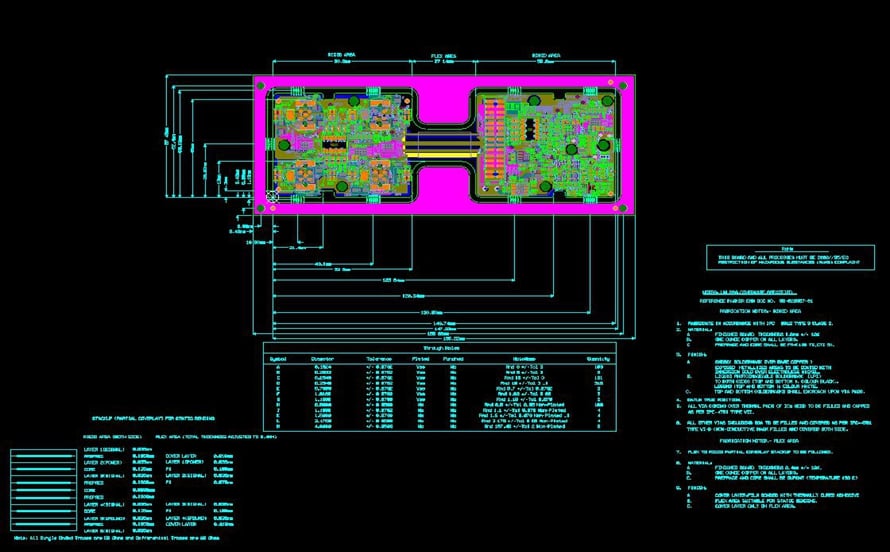
6. Fabrication Drawings
A fabrication drawing may specify:
- Board dimensions
- Thickness
- Tolerances
- Layer stackup
- Hole requirements
- Material
- Surface finish
- Special manufacturing requirements
7. Testing Instructions
Testing documentation defines how the finished PCB or PCBA should be verified.
Depending on the application, this may include:
- Electrical continuity testing
- ICT
- Functional testing
- Programming
- High-voltage testing
- Insulation testing
- Performance verification
8. Compliance Documentation
Depending on the application and target market, compliance information may be required for standards and regulations such as:
- RoHS
- REACH
- UL
- IPC requirements
- ISO-related quality requirements
- Industry-specific standards
The exact requirements depend on the product and destination market.
9. PCB Specification Documentation
A PCB specification document may include the technical requirements needed to reproduce the original board.
Typical specifications include:
PCB Thickness
Common PCB thicknesses include:
- 0.4 mm
- 0.6 mm
- 0.8 mm
- 1.0 mm
- 1.2 mm
- 1.6 mm
- 2.0 mm
- 2.4 mm
The correct thickness should be determined by the original design and mechanical requirements rather than selected solely from standard values.
Copper Thickness
Common copper thicknesses include approximately:
- 18 µm
- 35 µm
- 70 µm
- 105 µm
High-current applications may require significantly heavier copper.
Surface Finish
Possible PCB surface finishes include:
- HASL
- Lead-free HASL
- ENIG
- Immersion silver
- Immersion tin
- OSP
- Hard gold
- Gold fingers
The correct surface finish depends on electrical, mechanical, environmental, and assembly requirements.
Solder Mask Color
Common solder mask colors include:
- Green
- Black
- Red
- Blue
- White
The color itself usually has limited influence on electrical performance, but the selected solder mask system can affect manufacturing and inspection requirements.
PCB Material
Material specifications may include:
- FR-4
- High-Tg FR-4
- Metal-core materials
- Ceramic materials
- High-frequency laminates
- Flexible materials
Important material properties may include Tg, CTE, dielectric constant, dissipation factor, and CTI, depending on the application.
PCB Reverse Engineering Process
A professional PCB reverse engineering project normally follows a structured workflow.
Step 1: Obtain the Original PCB
The first step is to obtain a suitable reference board.
Ideally, the original PCB should be functional and physically intact. A working board makes it easier to verify electrical relationships and compare the reconstructed design.
If the board is damaged, multiple samples may be useful.
The engineer may document the board using high-resolution photographs, dimensional measurements, and detailed visual inspection.
Step 2: Document the PCB
Before modifying or disassembling the board, engineers should record its physical characteristics.
Important information includes:
- Overall dimensions
- Board thickness
- Mounting holes
- Connector locations
- Component locations
- Silkscreen markings
- Board-to-board interfaces
- Mechanical cutouts
- Reference designators
Both sides of the PCB should be documented carefully.
Step 3: Identify the Components
Each component should be identified as accurately as possible.
This may involve reading:
- Part numbers
- Package markings
- Manufacturer codes
- Component values
- Reference designators
The engineer may also use datasheets and component databases to determine the electrical characteristics of difficult-to-identify parts.
For obsolete components, equivalent or replacement components may need to be evaluated separately.
Step 4: Analyze the PCB Layers
Single-sided and double-sided boards can often be analyzed through direct visual inspection.
Multilayer boards are more complicated because internal copper layers cannot be directly observed.
Depending on the project, layer analysis may require:
- Cross-section analysis
- Microscopy
- X-ray inspection
- Microsectioning
- Electrical probing
- Specialized imaging techniques
The goal is to determine the internal layer structure, signal routing, power planes, ground planes, and via connections.
Step 5: Trace Electrical Connections
The next step is to reconstruct the electrical connectivity of the PCB.
Engineers may trace connections between:
- Component pins
- Pads
- Vias
- Copper traces
- Power planes
- Ground planes
- Connectors
Continuity testing with appropriate instruments can help determine whether two points are electrically connected.
For complex multilayer boards, electrical probing and other analytical techniques may be required.
Step 6: Reconstruct the Schematic
After component identification and net tracing, the electrical structure can be recreated in schematic design software.
The reconstructed schematic should represent:
- Components
- Component values
- Pin assignments
- Net names
- Power connections
- Ground connections
- Signal paths
At this stage, engineers should compare the reconstructed schematic against the original PCB to identify inconsistencies.
Step 7: Recreate the PCB Layout
Once the schematic is available, the physical PCB Design can be rebuilt.
The layout should reproduce the important characteristics of the original board, including:
- Board outline
- Component placement
- Mounting holes
- Connector locations
- Copper routing
- Via locations
- Keepout areas
- Solder mask openings
- Silkscreen
- Layer structure
However, an exact visual copy is not always necessary.
If the objective is to create a functionally equivalent replacement, the design may be optimized for modern manufacturing processes while maintaining the required electrical and mechanical characteristics.
Step 8: Generate Manufacturing Files
After the reconstructed PCB design has been verified, the required manufacturing files can be generated.
These may include:
- Gerber files
- Drill files
- Pick-and-place files
- BOM
- Assembly drawings
- Fabrication drawings
- Stackup information
- Special process documentation
The files should then undergo a manufacturing review before production.
Step 9: Perform DFM Verification
Design for Manufacturing (DFM) is particularly important when reproducing an older PCB.
The original board may have been designed according to manufacturing capabilities that are no longer available or economically practical.
A DFM review can evaluate:
- Trace width
- Trace spacing
- Hole sizes
- Annular rings
- Solder mask clearance
- Component spacing
- Panelization
- Manufacturing tolerances
- Surface finish
- Material availability
The goal is to ensure that the reconstructed design can be manufactured consistently.
Step 10: Manufacture and Test the PCB
After design verification, the PCB can enter the PCB Manufacturing process.
The first production run should be treated as a prototype or engineering validation stage whenever possible.
The new board should be compared with the original in terms of:
- Dimensions
- Component placement
- Electrical connections
- Interface compatibility
- Power consumption
- Signal behavior
- Functional performance
- Thermal behavior
For critical products, additional environmental, reliability, and safety testing may be required.
Challenges of PCB Reverse Engineering
PCB reverse engineering becomes increasingly difficult as PCB complexity increases.
Multilayer PCB Analysis
Internal copper layers cannot be directly inspected from the PCB surface. Specialized analytical methods may therefore be required.
Fine-Pitch Components
Modern BGA, QFN, LGA, and other fine-pitch packages can make visual inspection and electrical tracing more difficult.
Obsolete Components
If a component is no longer manufactured, engineers must determine whether an exact replacement exists or whether the circuit requires redesign.
High-Speed PCB Design
High-speed boards may require reconstruction of:
- Controlled impedance
- Differential pairs
- Length matching
- Reference planes
- Via transitions
- Return paths
Simply copying visible copper traces may not be sufficient to reproduce the original signal integrity.
RF and Microwave PCBs
RF designs require careful consideration of:
- Dielectric properties
- Trace geometry
- Impedance
- Grounding
- Transmission-line structures
- Connector transitions
A small change in geometry or material can affect RF performance.
HDI and Microvia Structures
HDI boards may use:
- Laser-drilled microvias
- Blind vias
- Buried vias
- Sequential lamination
- Fine-line routing
These structures can require advanced analysis before the original design can be accurately reconstructed.
PCB Reverse Engineering vs PCB Copying
The terms “PCB reverse engineering” and “PCB copying” are sometimes used interchangeably, but they can describe different levels of work.
PCB copying generally focuses on reproducing the physical and electrical characteristics of an existing PCB.
PCB reverse engineering is broader. It may involve reconstructing the schematic, identifying components, analyzing the layer stackup, recovering design intent, and creating new manufacturing documentation.
Therefore, a professional reverse-engineering project can provide more information than simply reproducing the visible appearance of a PCB.
How to Choose a PCB Reverse Engineering Service
When selecting a PCB reverse engineering provider, consider the company’s ability to handle both analysis and manufacturing.
Important capabilities include:
- PCB schematic reconstruction
- Component identification
- Multilayer PCB analysis
- High-density PCB analysis
- Gerber generation
- BOM reconstruction
- DFM review
- PCB prototyping
- PCB Manufacturing
- PCB Assembly
- Electrical testing
- Functional testing
It is also important to confirm whether the supplier can handle the PCB technology used in the original board.
For example, a simple two-layer FR-4 PCB and a high-speed 12-layer HDI PCB require very different reverse-engineering capabilities.
Legal and Intellectual Property Considerations
PCB reverse engineering should also be evaluated from a legal and intellectual-property perspective.
The fact that a person physically owns a PCB does not automatically mean that they have unrestricted rights to reproduce its design commercially.
Depending on the jurisdiction and project, issues may involve:
- Copyright
- Patents
- Trade secrets
- Design rights
- Contractual restrictions
- Licensing agreements
- Confidentiality obligations
Therefore, before reproducing a third-party PCB for commercial purposes, the customer should verify that the required rights and permissions are available.
For internal maintenance, interoperability, research, or replacement purposes, the applicable legal rules may differ by jurisdiction and circumstance.
Kingda PCB Reverse Engineering and Manufacturing Support
For customers who no longer have complete PCB design files, Kingda can support projects that require PCB analysis, design reconstruction, manufacturing, and assembly.
Depending on the project, the process can include:
Original PCB Analysis → Component Identification → Schematic Reconstruction → PCB Design → DFM Review → Gerber Generation → PCB Manufacturing → PCB Assembly → Testing
The exact workflow depends on PCB complexity, available reference boards, documentation, component availability, and required production quantity.
For multilayer, high-density, high-current, or specialized PCBs, the engineering team should evaluate the original board carefully before deciding on the appropriate reverse-engineering method.
Summary
PCB Reverse Engineering provides a practical approach for reproducing or redesigning PCBs when the original design documentation is incomplete, outdated, or unavailable.
A professional process can involve much more than copying visible traces. It may require physical measurement, component identification, electrical connectivity analysis, multilayer inspection, schematic reconstruction, PCB layout recreation, DFM verification, and prototype testing.
If the original Gerber files, schematic, BOM, drill files, assembly drawings, and manufacturing specifications are already available, reverse engineering may not be necessary. However, when these documents are missing, PCB reverse engineering can help recover the information required for modern PCB Design, PCB Manufacturing, and PCB Assembly.
The final objective should be to create a PCB that meets the required electrical, mechanical, thermal, manufacturing, and reliability specifications while maintaining compatibility with the intended product.