PCB Glossary: PCB Design, PCB Manufacturing & PCB Assembly Terminology
Understanding PCB Manufacturing, PCB Assembly, and electronic production starts with understanding the terminology used throughout the industry.
The PCB industry contains thousands of technical terms covering PCB materials, circuit design, fabrication processes, assembly technologies, testing methods, component packages, and quality standards. For engineers, purchasing teams, manufacturers, and newcomers to the electronics industry, understanding these terms can make communication with PCB suppliers much easier.
A complete PCB glossary could contain more than 1,000 terms, so it is not practical to list every technical definition in a single article. Instead, this guide focuses on some of the most commonly used terms in PCB Design, PCB Manufacturing, and PCB Assembly.
Basic PCB Terminology
The following terms describe the fundamental structures and features found on printed circuit boards.
| Term | Description |
|---|---|
| Printed Circuit Board (PCB) | A PCB is a board that mechanically supports and electrically connects electronic components through conductive copper patterns, pads, vias, and other structures. PCB may also be called a printed wiring board (PWB) or circuit board. |
| Layer | A PCB layer generally refers to a conductive copper layer or other functional layer within the board stackup. PCBs can range from single-layer boards to complex multilayer structures containing dozens of copper layers. |
| Dielectric | A dielectric is an electrically insulating material separating conductive layers. In a multilayer PCB, dielectric materials electrically isolate adjacent copper layers while providing mechanical support. |
| Trace / Conductor | A trace is a patterned copper conductor used to carry electrical signals or power between components, pads, vias, and other conductive structures. |
| Drilled Hole | A drilled hole is an opening created in a PCB through mechanical or laser drilling. Holes can be plated or non-plated and may serve electrical, mechanical, or assembly purposes. |
| PTH | PTH stands for Plated Through-Hole. A PTH contains a conductive copper-plated barrel extending through the PCB and can connect different copper layers or accommodate through-hole component leads. |
| NPTH | NPTH stands for Non-Plated Through-Hole. Unlike a PTH, an NPTH does not have a conductive plated barrel and is commonly used for mechanical mounting, alignment, or other non-electrical purposes. |
| Via | A via is a plated conductive structure used to establish an electrical connection between different PCB layers. Common types include through vias, blind vias, buried vias, microvias, stacked vias, and staggered vias. |
| Pad | A pad is a conductive copper area used to establish an electrical or mechanical connection. Pads are commonly used for SMT component soldering and through-hole component connections. |
| Outer Layer | The outer layers are the copper layers exposed on the top and bottom surfaces of a PCB. A double-sided PCB typically has two outer copper layers. |
| Inner Layer | Inner layers are copper layers located inside a multilayer PCB. They are not directly exposed on the board surface and are commonly used for signal routing, power planes, and ground planes. |
| Copper Thickness | Copper thickness refers to the thickness of the copper foil or plated copper on a PCB. Common starting copper weights include 0.5 oz, 1 oz, and 2 oz, while heavy-copper designs may use much greater copper thicknesses. |
| PCB Thickness | PCB thickness refers to the overall finished thickness of the board, including copper, dielectric materials, solder mask, and other layers. 1.6 mm is a common nominal thickness, but thinner and thicker boards are widely available. |
| Solder Mask | Solder mask is a protective polymer coating applied over selected areas of the PCB to protect copper from contamination and oxidation and to reduce the risk of solder bridging. Green is the most common color, but many other colors are available. |
| Silkscreen | Silkscreen is printed identification information on the PCB surface. It can include reference designators, polarity markings, logos, labels, warnings, and other assembly information. |
| Surface Finish | Surface finish is the protective finish applied to exposed copper pads to improve solderability and protect the copper surface. Common finishes include HASL, ENIG, ENEPIG, OSP, immersion silver, and immersion tin. |
| Tooling Hole | A tooling hole is a mechanical reference hole used to position or secure a PCB or panel during manufacturing and assembly processes. |
| Routing | Routing can refer to electrical trace routing during PCB Design or mechanical routing, where a milling cutter is used to separate individual PCB outlines from a production panel. |
| Punching | Punching uses a dedicated press and tooling die to separate certain PCB shapes from a panel. It is particularly suitable for high-volume production of boards with compatible shapes and materials. |
| V-Scoring | V-scoring, or V-grooving, creates controlled V-shaped grooves between adjacent boards in a panel. The individual PCBs can later be separated along the scored lines. |
PCB Substrate and Material Glossary
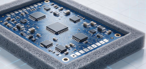
PCB materials have a direct influence on electrical performance, thermal behavior, mechanical strength, reliability, and manufacturing cost.
| Term | Description |
|---|---|
| Copper-Clad Laminate (CCL) | CCL is a fundamental material used to manufacture PCBs. It consists of a dielectric substrate laminated with copper foil on one or both sides. FR-4 CCL, high-Tg CCL, flexible CCL, and high-frequency laminates are common examples. |
| Metal-Core Material | Metal-core PCB materials typically contain a metal base, a dielectric thermal layer, and a copper circuit layer. Aluminum-core PCBs are widely used for LED lighting and other thermal-management applications. |
| Core | A core is a rigid dielectric material with copper foil laminated to one or both sides. Cores form an important part of multilayer PCB stackups. |
| Prepreg | Prepreg is a resin-impregnated reinforcement material used to bond PCB layers together during multilayer lamination. Its final thickness depends on resin content, glass style, lamination pressure, and process conditions. |
| Adhesive Film | Adhesive films are used in flexible PCB construction to bond coverlayers, stiffeners, or flexible circuit layers. Materials can include polyimide-based and other specialized adhesive systems. |
| Coverlay | Coverlay is a flexible protective layer used primarily on flexible circuits. It protects copper traces and provides insulation in areas where solder mask is not used. Polyimide is a common coverlay material. |
| Stiffener | A stiffener is attached to selected areas of a flexible PCB to increase mechanical rigidity. FR-4, polyimide, and metal stiffeners may be used depending on the application. |
| FR-4 | FR-4 is a widely used PCB laminate system based on glass fiber reinforcement and epoxy resin. It provides a combination of electrical insulation, mechanical strength, thermal stability, and cost effectiveness. |
| Polyimide (PI) | Polyimide is a flexible and thermally stable material widely used in flexible PCBs and rigid-flex PCBs. It can withstand repeated flexing when the appropriate flexible construction is used. |
| Ceramic Material | Ceramic PCB materials can provide high thermal conductivity, dimensional stability, and electrical performance. They are used in demanding applications such as high-power electronics, RF systems, and high-temperature environments. |
| PTFE | Polytetrafluoroethylene (PTFE) is a low-loss dielectric material used in specialized high-frequency and microwave PCBs. PTFE laminates are selected for their electrical characteristics rather than simply their thermal properties. |
PCB Manufacturing Terminology
The following terms are frequently used during PCB fabrication and advanced PCB manufacturing.
Countersink
A countersink is a conical enlargement around a hole that allows a flat-head screw to sit flush with or below the PCB surface.
Depending on the mechanical design, a countersunk hole may require specialized drilling or routing operations.
Peelable Solder Mask
Peelable solder mask is a temporary protective material applied to selected PCB areas that must remain free from solder during assembly.
It can protect specific pads, contacts, or holes during soldering and is removed after the relevant process.
Carbon Ink
Carbon ink is a conductive material printed onto selected PCB areas.
It can be used for applications such as:
- Keypad contacts
- Membrane-switch interfaces
- Carbon resistors
- Wear-resistant conductive surfaces
The electrical resistance of carbon ink can be controlled according to the application requirements.
Gold Fingers
Gold fingers are exposed contact pads along the edge of a PCB that are used to connect the board to a mating connector.
They are typically manufactured using a suitable hard-gold plating system to withstand repeated insertion and removal.
Common applications include:
- Computer expansion cards
- Memory modules
- Industrial control cards
- Communication boards
Blind Via
A blind via connects an outer PCB layer to one or more inner layers without passing completely through the board.
For example, in a six-layer PCB, a blind via may connect Layer 1 to Layer 2, Layer 3, or another designated inner layer depending on the manufacturing process.
Buried Via
A buried via connects internal PCB layers without extending to the outer surface.
Because buried vias are completely enclosed within the PCB, they are commonly used in high-density multilayer designs.
HDI
HDI stands for High-Density Interconnect.
HDI PCBs use advanced interconnection structures such as microvias, fine-line traces, fine-pitch pads, sequential lamination, and sometimes stacked or staggered microvias.
HDI technology allows engineers to achieve greater routing density within a smaller PCB footprint.
Stacked Microvia
A stacked microvia is positioned directly above another microvia in a multilayer HDI structure.
Stacked microvias can provide vertical interconnections between multiple layers while reducing routing space.
Staggered Microvia
Staggered microvias are arranged with an offset rather than being directly aligned vertically.
This structure can simplify certain HDI manufacturing processes and improve manufacturing reliability depending on the stackup.
Any-Layer HDI
Any-layer HDI is an advanced HDI structure in which microvias can be formed between multiple adjacent layers throughout the PCB stackup.
This approach can provide very high routing density for compact and sophisticated electronic products.
Backdrilling
Backdrilling is a controlled-depth drilling process used to remove an unwanted portion of a plated through-hole barrel.
In high-speed multilayer PCBs, the unused portion of a via can behave as a stub and negatively affect signal integrity.
Backdrilling removes part of that stub while leaving the required electrical connection intact.
Via-in-Pad
Via-in-pad places a via directly within a component pad.
This technology is commonly used in high-density PCB and HDI designs, especially with fine-pitch BGA packages.
To prevent solder from flowing into the via and creating assembly defects, the via generally requires an appropriate filling and capping process.
RF and Microwave PCB
RF stands for radio frequency, while microwave generally refers to higher-frequency electromagnetic applications.
RF and microwave PCBs require careful control of:
- Dielectric properties
- Trace geometry
- Impedance
- Grounding
- Transmission-line structures
- Copper roughness
- Layer spacing
The exact frequency range depends on the application, so RF and microwave should not be defined by one universal frequency boundary.
Via Filling
Via filling refers to filling a via with a suitable material such as resin or conductive material.
Via filling is especially important for via-in-pad structures and certain HDI applications.
After filling, additional processing such as planarization and copper capping may be required depending on the design.
Heavy Copper PCB
A Heavy Copper PCB uses significantly thicker copper than standard PCB constructions.
Standard PCB copper commonly starts around 1 oz, equivalent to approximately 35 µm before additional plating. Heavy-copper designs may use several ounces of copper and can be engineered for high-current and high-power applications.
Ultra-heavy copper constructions can reach very high copper weights, but the achievable thickness depends on the PCB manufacturer’s process capability.
Controlled Impedance
Controlled impedance is the practice of designing and manufacturing PCB transmission lines so that their characteristic impedance remains within a specified range.
Common impedance types include:
- Single-ended impedance
- Differential impedance
Impedance depends on factors such as:
- Trace width
- Trace thickness
- Dielectric thickness
- Dielectric constant
- Reference-plane configuration
Controlled impedance is especially important in high-speed digital, RF, microwave, telecommunications, and high-performance computing applications.
Flexible PCB
A flexible PCB, or FPCB, uses flexible dielectric materials that allow the circuit to bend.
Flexible PCBs are widely used where space, weight, and mechanical movement are important.
Applications include:
- Smartphones
- Cameras
- Wearable electronics
- Medical devices
- Consumer electronics
- Automotive electronics
Rigid-Flex PCB
A rigid-flex PCB combines rigid PCB sections with flexible circuit sections in a single integrated structure.
This construction can provide both mechanical support for components and flexibility for interconnections.
Rigid-flex PCBs are widely used in:
- Aerospace electronics
- Medical equipment
- Industrial systems
- Automotive electronics
- Portable electronics
- High-density electronic products
Backplane PCB
A backplane is a large PCB or wiring structure designed to interconnect multiple daughtercards or plug-in modules.
Backplanes often contain many high-speed interfaces and require careful signal-integrity design.
Depending on the application, they may use:
- High-Tg materials
- Low-loss laminates
- Controlled impedance
- Advanced multilayer stackups
- Press-fit connectors
High-speed backplanes can contain many layers and require precise manufacturing and testing.
Basic PCB Assembly Terminology
PCB Assembly, or PCBA manufacturing, involves mounting electronic components onto a fabricated bare PCB.
The following terms are among the most common.
| Term | Description |
|---|---|
| PCBA | PCBA stands for Printed Circuit Board Assembly. It refers to a bare PCB populated with electronic components and soldered connections. |
| SMT | Surface-Mount Technology is an assembly technology in which components are mounted directly onto PCB surface pads. |
| THT / PTH Assembly | Through-Hole Technology uses component leads that pass through PCB holes and are soldered to pads. |
| Solder Paste | Solder paste is a mixture of fine solder alloy particles and flux formulated for stencil printing and SMT assembly. It is printed onto PCB pads before component placement and reflow soldering. |
| Pick-and-Place Machine | A pick-and-place machine automatically picks electronic components from feeders and places them onto PCB pads with high speed and precision. |
| BOM | BOM stands for Bill of Materials. It lists the components required for PCB assembly, including part numbers, quantities, values, packages, and other sourcing information. |
| Gerber Files | Gerber files are widely used to communicate PCB fabrication artwork and related manufacturing information to PCB manufacturers. |
| Reflow Soldering | Reflow soldering uses a controlled thermal profile to melt solder paste and form solder joints between SMT components and PCB pads. |
| Wave Soldering | Wave soldering uses a controlled wave of molten solder to solder suitable through-hole components and other compatible joints. |
| AOI | Automated Optical Inspection uses cameras and software to inspect assembled PCBs for defects such as missing, misplaced, incorrectly oriented, or improperly soldered components. |
| ICT | In-Circuit Test checks electrical characteristics and connectivity of an assembled PCB. It can detect issues such as opens, shorts, component problems, and certain assembly defects. |
| FCT | Functional Circuit Test, commonly called Functional Test, evaluates whether the completed PCBA performs according to its intended electrical and functional requirements. |
| X-Ray Inspection | X-ray inspection allows manufacturers to inspect hidden solder joints and internal structures that cannot be adequately evaluated through conventional optical inspection. It is particularly useful for BGA, QFN, bottom-terminated components, and other concealed solder connections. |
Common PCB Assembly Terms Explained
SMT Assembly
SMT assembly mounts components directly onto PCB pads.
Because SMT components are compact and can be placed at high density, SMT is the dominant assembly method for many modern electronic products.
Through-Hole Assembly
Through-hole assembly inserts component leads through drilled PCB holes.
This method is often selected for components requiring additional mechanical strength, such as connectors, transformers, relays, and certain power components.
Reflow Soldering
During reflow soldering, solder paste is printed onto PCB pads before SMT components are placed.
The assembled PCB then passes through a controlled reflow oven where the solder paste melts and solidifies to create solder joints.
Wave Soldering
Wave soldering is primarily used for through-hole assembly.
The PCB passes over a controlled wave of molten solder, allowing solder to contact the exposed leads and pads on the underside of the board.
Automated Optical Inspection (AOI)
AOI uses cameras and image-processing software to inspect PCB assemblies automatically.
Typical AOI defects include:
- Missing components
- Incorrect component orientation
- Component misalignment
- Solder bridges
- Insufficient solder
- Excessive solder
- Soldering defects
AOI can improve inspection speed and consistency compared with relying entirely on manual visual inspection.
In-Circuit Test (ICT)
ICT is an electrical test method used to verify individual components and electrical connections on a PCBA.
A dedicated fixture and test program are commonly required.
ICT can identify:
- Open circuits
- Short circuits
- Incorrect component values
- Missing components
- Certain solder defects
- Incorrect electrical connections
Functional Test (FCT)
Functional testing evaluates whether the assembled PCB performs its intended function.
Depending on the product, an FCT system may verify:
- Voltage
- Current
- Communication
- Sensor operation
- Motor control
- Display functions
- Input/output behavior
- System-level performance
Unlike ICT, which focuses heavily on circuit-level verification, functional testing evaluates the operational behavior of the finished assembly.
X-Ray Inspection
X-ray inspection is used when solder joints or internal structures cannot be adequately inspected from the PCB surface.
It is particularly useful for:
- BGA packages
- QFN packages
- Bottom-terminated components
- Hidden solder joints
- Voids
- Internal interconnections
X-ray inspection can therefore complement AOI and visual inspection in advanced PCB Assembly.
Why Understanding PCB Terminology Matters
Understanding PCB terminology helps engineers, purchasing teams, designers, and manufacturers communicate more efficiently.
For example, simply specifying “a multilayer PCB” is not enough for production.
A manufacturer may also need to know:
- Layer count
- PCB thickness
- Copper weight
- Material
- Tg
- Surface finish
- Solder mask
- Controlled impedance requirements
- Hole structure
- Minimum trace width
- Minimum spacing
- Special manufacturing requirements
Similarly, a PCBA quotation requires much more than the PCB Gerber files. The manufacturer may need the BOM, pick-and-place data, assembly drawings, component specifications, and testing requirements.
Clear terminology reduces misunderstandings and helps ensure that the final product meets the intended PCB Design and manufacturing requirements.
PCB Design, Manufacturing, and Assembly Workflow
Understanding how these terms connect to one another is equally important.
A typical electronic manufacturing workflow can be summarized as:
PCB Design → Engineering Review → Gerber Generation → PCB Manufacturing → Bare PCB Inspection → Component Sourcing → SMT/THT Assembly → Reflow/Wave/Selective Soldering → AOI/X-Ray → ICT/FCT → Final Inspection
Each stage uses its own technical vocabulary.
For example:
- PCB Design defines the electrical and physical structure.
- Gerber files communicate fabrication data.
- CCL and core materials determine the PCB substrate structure.
- Prepreg helps form multilayer constructions.
- PTH and vias create electrical interconnections.
- Solder mask protects selected copper areas.
- Surface finish protects exposed pads.
- SMT and THT define component assembly methods.
- Reflow and wave soldering create solder joints.
- AOI, ICT, and FCT verify assembly quality and functionality.
Understanding these relationships makes it much easier to communicate with a PCB manufacturer or PCBA supplier.
Kingda PCB Manufacturing and PCB Assembly
For customers who require complete electronic manufacturing support, Kingda can support projects across PCB Design, PCB fabrication, PCB Assembly, and testing.
Depending on the product requirements, the manufacturing process may involve:
- Standard FR-4 PCB
- High-Tg PCB
- HDI PCB
- Heavy Copper PCB
- Aluminum PCB
- Flexible PCB
- Rigid-Flex PCB
- High-speed PCB
- RF and microwave PCB
- SMT Assembly
- Through-Hole Assembly
- Reflow Soldering
- Wave Soldering
- AOI
- X-Ray Inspection
- ICT
- Functional Testing
A clear understanding of PCB terminology allows customers and manufacturers to define technical requirements more precisely and reduce potential errors during engineering review and production.
Summary
PCB terminology covers almost every aspect of electronic hardware development, from PCB Design and material selection to PCB Manufacturing, assembly, inspection, and testing.
Terms such as PCB, dielectric, trace, pad, PTH, NPTH, via, solder mask, surface finish, CCL, core, prepreg, FR-4, HDI, backdrilling, controlled impedance, PCBA, SMT, THT, reflow soldering, wave soldering, AOI, ICT, FCT, and X-ray inspection are fundamental to modern PCB production.
Although this glossary cannot cover every technical term used in the PCB industry, it provides a practical foundation for understanding the terminology most commonly encountered during PCB design, fabrication, assembly, and quality control.
As PCB technology becomes increasingly sophisticated, especially in HDI, high-speed, RF, flexible, rigid-flex, and high-power applications, understanding the correct terminology becomes even more important for successful communication between engineers, manufacturers, suppliers, and customers.