2-Layer PCB Stackup: PCB Design, PCB Manufacturing & Layer Stackup Guide
Printed circuit boards (PCBs) are the foundation of countless electronic and electrical products, ranging from simple control circuits to highly complex computing and communication systems. PCBs are available in different sizes, shapes, materials, and layer configurations depending on their electrical and mechanical requirements.
A simple PCB may contain only one or two copper layers, while advanced products can use dozens of conductive layers. Among these configurations, the 2-Layer PCB Stackup remains one of the most common and practical options for low- to moderate-complexity electronic products.
For engineers who are new to PCB Design, a two-layer board is often one of the first multilayer configurations to learn. Understanding how a two-layer stackup works also provides a foundation for understanding more complex four-layer, six-layer, and HDI PCB structures.
This article explains what a 2-layer PCB stackup is, common stackup configurations, their advantages and limitations, design considerations, and typical applications.
What Is a 2-Layer PCB Stackup?
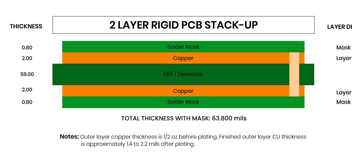
A 2-Layer PCB Stackup is a PCB construction consisting of two copper layers separated by a dielectric substrate.
A typical two-layer PCB contains:
- Top copper layer
- Dielectric core
- Bottom copper layer
The copper layers are used for signal routing, power distribution, and ground connections. Components can be mounted on either or both sides of the board, depending on the design.
Unlike a single-layer PCB, a two-layer PCB can use plated through-holes and vias to connect electrical networks between the top and bottom copper layers.
This additional routing capability makes two-layer PCBs significantly more versatile than single-layer boards.
A basic two-layer construction can be represented as:
Top Copper → Dielectric Core → Bottom Copper
The dielectric material is commonly FR-4 for conventional applications, although other materials can be used for specialized flexible, RF, thermal, or high-performance designs.
Common 2-Layer PCB Stackup Configurations
Compared with four-layer or higher-layer PCBs, two-layer boards have relatively few stackup options. Nevertheless, the way the two copper layers are assigned can have a significant effect on signal integrity, grounding, routing density, and manufacturability.
Two common approaches are described below.
Type I: Signal – Signal

In a signal-signal configuration, both copper layers are primarily used for routing.
Components may be placed on either side of the PCB, allowing designers to make better use of the available board area.
This approach is practical for relatively simple circuits where high-speed signal integrity is not the primary concern.
For example, low-speed interfaces such as:
- GPIO
- UART
- Simple control signals
- Basic sensor interfaces
- Low-speed analog circuits
can often be implemented successfully on a two-layer signal-routing structure.
However, designers should carefully consider the return-current path.
A high-frequency signal does not simply travel along a trace from the source to the load. Its return current also needs a controlled path. If a continuous reference plane is unavailable, the return current may need to travel around discontinuities, increasing loop area and potentially increasing EMI, crosstalk, and signal-integrity problems.
Therefore, although a signal-signal stackup can work well for low-speed circuits, it becomes increasingly difficult to control signal integrity as edge rates and operating frequencies increase.
Type II: Signal – Ground

A signal-ground configuration dedicates one copper layer primarily to ground while the other layer is used mainly for signal routing and component placement.
For example:
Top Layer → Components + Signals
Bottom Layer → Ground Plane
This configuration can provide a much more controlled return-current path than a signal-signal arrangement.
A continuous ground plane can help:
- Reduce signal loop area
- Improve return-current continuity
- Reduce electromagnetic radiation
- Improve signal integrity
- Simplify grounding
- Support controlled-impedance routing
This makes the signal-ground configuration attractive for applications where signal integrity is more important but the circuit complexity does not justify a four-layer PCB.
The main limitation is routing density. Because one layer is primarily reserved for ground, less copper area is available for signal routing.
However, this tradeoff can often be worthwhile for simple communication, sensor, control, and mixed-signal circuits.
2-Layer PCB Stackup Materials
The dielectric core is a critical part of a two-layer PCB.
For general-purpose applications, FR-4 is the most common substrate material because it offers a good balance between:
- Cost
- Mechanical strength
- Electrical insulation
- Thermal performance
- Availability
- Manufacturability
For specialized applications, other materials may be used.
Examples include:
- Polyimide for flexible PCBs
- High-frequency laminates for RF applications
- Aluminum-based materials for thermal management
- Ceramic materials for high-temperature or high-frequency applications
Because a two-layer PCB has only one dielectric core between its copper layers, the core thickness is a major factor in determining the finished PCB thickness.
Typical design parameters include:
- Core thickness
- Copper thickness
- Dielectric constant
- Dielectric loss
- Finished board thickness
- Surface finish
- Solder mask thickness
For conventional PCB Manufacturing, the exact material and thickness should be selected according to the electrical, mechanical, thermal, and manufacturing requirements of the product.
2-Layer PCB Stackup and Controlled Impedance
One common misconception is that controlled impedance is impossible on a two-layer PCB. In reality, controlled impedance can be implemented on a two-layer board under suitable conditions.
However, achieving stable impedance can be more difficult than on a multilayer PCB with dedicated reference planes.
For example, a microstrip transmission line can be formed using:
Signal Trace → Dielectric → Ground Plane
The impedance depends on factors such as:
- Trace width
- Copper thickness
- Dielectric thickness
- Dielectric constant
- Distance to the reference plane
- Trace geometry
- Copper surface characteristics
A signal-ground two-layer configuration is therefore much more suitable for controlled impedance than a signal-signal configuration.
However, designers should not assume that every two-layer PCB can reliably support high-speed impedance-controlled interfaces.
For demanding high-speed designs, four-layer or higher-layer stackups generally provide more flexibility for signal routing, reference planes, power distribution, and EMI control.
Why Is a Ground Plane Important on a 2-Layer PCB?
A continuous ground plane can significantly improve the electrical behavior of a two-layer PCB.
When a signal trace is routed above a continuous ground plane, its return current tends to follow a path close to the signal trace.
This reduces the effective current-loop area.
A smaller loop area can help reduce:
- EMI
- Crosstalk
- Ground noise
- Signal distortion
- Unwanted radiation
For this reason, designers should avoid unnecessarily cutting or splitting the ground plane underneath critical signal traces.
When a signal must transition between layers, designers should also consider the return-current path and place appropriate ground vias when necessary.
Advantages of a 2-Layer PCB Stackup
A two-layer PCB provides several advantages, which explains why it remains widely used in electronic products.
Lower Cost
One of the biggest advantages is cost.
A two-layer PCB generally costs significantly less than a four-layer or higher-layer board because it requires fewer conductive layers and a simpler manufacturing process.
This makes it attractive for:
- Consumer electronics
- Industrial controls
- Simple IoT devices
- LED products
- Development boards
- Low-complexity controllers
Simple Manufacturing Process
The manufacturing process for a two-layer PCB is relatively straightforward.
Most PCB manufacturers can produce standard two-layer boards, making them widely available.
A simpler structure can also help reduce manufacturing lead time and simplify production planning.
Easier PCB Design
Two-layer boards have fewer routing constraints than high-layer-count boards in terms of stackup management.
For beginners, this makes them useful for learning:
- Schematic-to-PCB workflows
- Component placement
- Trace routing
- Grounding
- Via usage
- Design-rule checking
- Gerber generation
Vias Can Be Used
Unlike single-layer PCBs, two-layer PCBs can use vias to connect the top and bottom copper layers.
This gives designers considerably more routing flexibility.
Through vias can be used to:
- Change signal layers
- Connect ground
- Connect power
- Reduce routing congestion
Components Can Be Mounted on Both Sides
Components can be placed on either side of a two-layer PCB.
This can increase component density and reduce the overall board size compared with placing all components on one side.
However, component placement must be planned according to the assembly process.
Suitable for Many Flexible PCB Designs
Two-layer structures are also widely used for flexible circuits.
A flexible PCB can use a two-conductor-layer construction with a flexible dielectric such as polyimide.
The exact construction depends on whether the circuit is single-sided, double-sided, or multilayer flexible.
Disadvantages of a 2-Layer PCB Stackup
Despite its advantages, a two-layer PCB has several limitations.
Limited Routing Density
Only two copper layers are available for routing.
As circuit complexity increases, designers may quickly run out of routing space.
This is particularly challenging when the board contains:
- Large numbers of components
- Fine-pitch ICs
- Multiple power rails
- High-speed interfaces
- Dense analog circuitry
- Multiple ground domains
In such cases, increasing the layer count may be more practical.
More Difficult High-Speed Design
Two-layer PCBs can support certain high-speed interfaces, but high-speed performance depends on the signal edge rate, transmission-line geometry, stackup, reference-plane continuity, connector structures, and overall design.
It is therefore inaccurate to define a universal frequency threshold at which a two-layer PCB becomes unusable.
For demanding high-speed designs, four-layer or higher-layer boards are often preferred because they make it easier to provide continuous reference planes and controlled signal-routing structures.
More Difficult EMI Control
Without dedicated internal reference planes, EMI management can be more challenging.
Poor grounding and large return-current loops can increase electromagnetic radiation and susceptibility.
Limited Power Distribution
A two-layer PCB does not have dedicated internal power planes.
Power and ground must share the available copper layers with signal routing.
For high-current applications, designers may therefore need:
- Wider copper traces
- Copper pours
- Larger vias
- Multiple parallel vias
- Heavier copper
- Dedicated power-routing areas
Limited Space for Complex Circuits
As the number of components and connections increases, a two-layer PCB may require a larger physical area.
Increasing the board size can eventually become more expensive or mechanically impractical than adding PCB layers.
2-Layer PCB vs. 4-Layer PCB
The choice between two-layer and four-layer construction depends primarily on circuit complexity and electrical requirements.
| Feature | 2-Layer PCB | 4-Layer PCB |
|---|---|---|
| Copper layers | 2 | 4 |
| Manufacturing cost | Lower | Higher |
| Routing density | Limited | Higher |
| Ground-plane management | More challenging | Easier |
| Power distribution | Limited | Better |
| EMI control | More challenging | Generally easier |
| High-speed design | Possible for suitable designs | More flexible |
| Controlled impedance | Possible | More practical |
| Board size | May need to be larger | Can often be smaller |
| Design complexity | Lower | Higher |
| Typical applications | Simple to moderate circuits | Moderate to complex circuits |
A four-layer PCB commonly uses a structure such as:
Signal – Ground – Power – Signal
or another stackup optimized for the specific application.
The additional layers provide more routing space and dedicated reference structures.
PCB Design Considerations for 2-Layer Stackups
Successful PCB Design requires more than simply placing two copper layers on a dielectric core.
Component Placement
Component placement should be completed before detailed routing begins.
Critical considerations include:
- Functional grouping
- Signal flow
- Power distribution
- Thermal requirements
- Connector locations
- Assembly access
- Test-point accessibility
Ground Plane Design
Whenever possible, maintain a large and continuous ground copper area.
Avoid unnecessary slots or cuts underneath sensitive signal traces.
Short Return Paths
High-speed or fast-edge signals require short and predictable return paths.
Designers should avoid routing signals across gaps in the reference plane.
Trace Width
Trace width should be selected according to:
- Current requirements
- Copper thickness
- Temperature rise
- Manufacturing capability
- Impedance requirements
Power traces may require significantly greater width than low-current signal traces.
Via Placement
Vias should be used strategically.
Excessive vias can consume valuable routing space, while insufficient vias may make the design difficult to complete.
Ground stitching vias can also help connect copper regions and improve return-current paths.
Thermal Management
Power components can generate significant heat.
A two-layer PCB may use:
- Large copper areas
- Thermal vias
- Copper pours
- External heat sinks
- Heavier copper
- Thermal interface structures
The appropriate solution depends on the power level and thermal environment.
2-Layer PCB Manufacturing Process
The PCB Manufacturing process for a standard two-layer board generally includes:
- Material preparation
- Inner/outer artwork preparation
- Copper imaging
- Etching
- Drilling
- Hole-wall preparation
- Electroless copper deposition
- Copper electroplating
- Solder mask application
- Surface finish
- Silkscreen printing
- Electrical testing
- Routing or V-scoring
- Final inspection
- Packaging
Although a two-layer PCB is simpler than a multilayer PCB, manufacturing quality still depends on accurate drilling, plating, trace formation, solder mask registration, surface finish, and electrical testing.
Applications of 2-Layer PCB Stackups
Two-layer PCBs are widely used in applications where circuit density and signal-integrity requirements are moderate.
LED PCB
LED control boards and simple LED lighting circuits often use two-layer PCBs.
When the LED spacing and circuit complexity are relatively low, two copper layers can provide sufficient routing capacity.
For high-power LED applications, however, thermal requirements may lead designers toward aluminum-based or other thermally enhanced PCB structures.
Development Boards
Many MCU development boards, evaluation boards, and prototype circuits can be implemented using two-layer PCBs.
Their low manufacturing cost makes them useful for:
- Prototyping
- Educational projects
- Product development
- Circuit evaluation
- Small-batch production
Simple Switching Power Supplies
Some relatively simple switching power supplies can use two-layer PCBs.
However, power electronics require careful attention to:
- High-current loops
- Switching-node area
- Grounding
- Creepage and clearance
- Thermal management
- EMI
- Component placement
A two-layer structure should therefore only be selected when it can satisfy the electrical and safety requirements of the specific power circuit.
Industrial Control Boards
Simple control boards for sensors, switches, relays, and actuators can often be implemented using two-layer construction.
Consumer Electronics
Simple consumer electronic products can also use two-layer PCBs when the circuit density and performance requirements are compatible with the available routing space.
When Should You Use a 2-Layer PCB?
A two-layer PCB is generally appropriate when:
- The circuit has relatively low or moderate complexity.
- Routing can be completed with two copper layers.
- High-density interconnects are not required.
- The signal-return paths can be controlled adequately.
- Cost is an important design consideration.
- The product does not require complex multilayer power distribution.
- The mechanical size can accommodate the required routing area.
A four-layer or higher-layer PCB should be considered when the design requires:
- Dense routing
- Multiple power domains
- Dedicated ground planes
- High-speed interfaces
- Complex impedance control
- Better EMI management
- Smaller board dimensions
- Advanced digital or RF functionality
The decision should ultimately be based on electrical, mechanical, thermal, manufacturing, and cost requirements rather than layer count alone.
Conclusion
The 2-Layer PCB Stackup remains one of the most widely used PCB configurations because it provides a practical balance between cost, manufacturability, routing flexibility, and electrical performance.
A basic two-layer PCB consists of two copper layers separated by a dielectric core. Designers can use both layers for signal routing or dedicate one layer primarily to ground to improve signal integrity and return-current control.
Although two-layer PCBs have limitations in routing density, power distribution, EMI control, and demanding high-speed applications, they remain an excellent choice for many low- and medium-complexity products.
For successful PCB Design, engineers should carefully consider component placement, grounding, return-current paths, trace width, via placement, thermal management, and impedance requirements. During PCB Manufacturing, material selection, drilling, plating, solder mask, surface finish, and electrical testing must also be properly controlled.
The key is not to automatically choose the highest possible layer count. Instead, select the simplest PCB stackup that can reliably satisfy the product’s electrical, mechanical, thermal, and manufacturing requirements.
Article Summary
A 2-layer PCB stackup consists of two copper layers separated by a dielectric core and is widely used in simple to moderately complex electronic products. It offers low cost, straightforward manufacturing, easy prototyping, and sufficient routing flexibility for many applications. However, as routing density, high-speed requirements, EMI constraints, and power-distribution complexity increase, a four-layer or higher-layer PCB may provide a more practical solution.