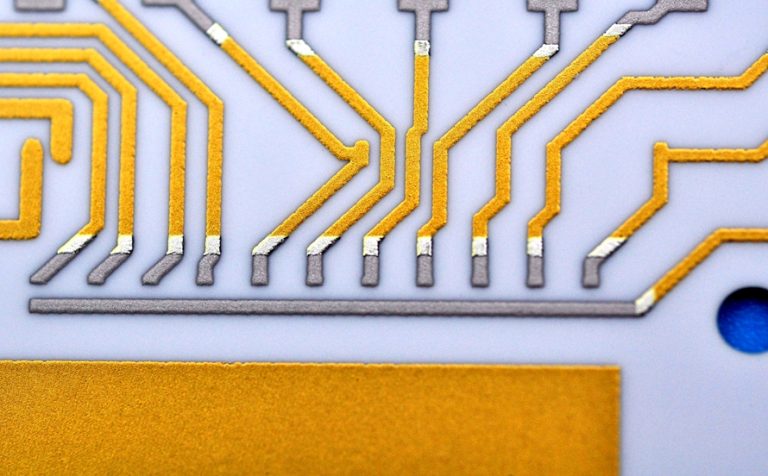
Alumina PCB: PCB Design, PCB Manufacturing & Ceramic PCB Guide
As modern electronic devices continue to become more powerful and compact, thermal management has become an increasingly important consideration in PCB Design. Standard FR-4 PCBs provide a cost-effective solution for a wide range of applications, but their relatively low thermal conductivity can become a limitation in high-power and high-temperature environments.
For applications that require efficient heat dissipation, electrical insulation, dimensional stability, and resistance to elevated temperatures, an Alumina PCB can be a suitable alternative.
An alumina PCB is a type of Ceramic PCB that uses aluminum oxide (Al₂O₃) as the substrate instead of conventional glass-fiber-reinforced epoxy materials such as FR-4. Depending on the manufacturing technology and application, alumina substrates can be metallized using direct bonded copper (DBC), direct plated copper (DPC), thin-film, or thick-film processes.
Because alumina combines good thermal conductivity with excellent electrical insulation, mechanical strength, chemical stability, and relatively low thermal expansion, it is widely used in power electronics, LED lighting, automotive electronics, RF and microwave circuits, industrial equipment, and other demanding applications.
This guide explains what an alumina PCB is, its major substrate types, design considerations, manufacturing processes, advantages and limitations, applications, cost factors, and how to select an appropriate Alumina PCB Manufacturer.
What Is an Alumina PCB?
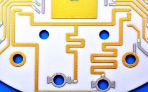
An Alumina PCB is a ceramic printed circuit board that uses aluminum oxide (Al₂O₃) as its insulating substrate.
Unlike conventional FR-4, which consists primarily of glass fiber reinforced with epoxy resin, alumina is an inorganic ceramic material. This gives alumina PCBs a different combination of electrical, thermal, and mechanical properties.
Key characteristics include:
- High electrical insulation
- Good thermal conductivity
- Low moisture absorption
- High temperature resistance
- Good dimensional stability
- High mechanical hardness
- Chemical stability
- Relatively low coefficient of thermal expansion (CTE)
Alumina is one of the most widely used ceramic substrate materials because it provides a practical balance between thermal performance, electrical insulation, mechanical properties, manufacturability, and cost.
It is important to distinguish an alumina PCB from an aluminum PCB. An aluminum PCB normally uses a metal core for thermal management, while an alumina PCB uses ceramic aluminum oxide as the electrical insulating substrate.
Types of Alumina PCB Substrates
Alumina ceramic substrates are commonly classified according to their Al₂O₃ purity. Common grades include 96%, 99%, and 99.5% or 99.6% alumina.
The exact electrical, thermal, mechanical, and processing properties depend on the manufacturer’s material formulation and datasheet, so values should always be confirmed for the specific ceramic grade being used.
96% Alumina PCB
96% alumina is widely used for ceramic electronic substrates and thick-film applications.
Its advantages include:
- Good electrical insulation
- Good thermal conductivity
- Good mechanical strength
- Relatively economical ceramic construction
- Compatibility with thick-film metallization
It is frequently used for power electronics, hybrid circuits, LED applications, sensors, and general ceramic electronic substrates.
99% Alumina PCB
Higher-purity alumina generally provides improved material performance in demanding applications.
It can offer:
- Higher temperature capability
- High mechanical strength
- Excellent electrical insulation
- Good chemical stability
- Low moisture absorption
Applications may include high-temperature electronics, industrial equipment, and specialized electronic substrates.
99.5%–99.6% Alumina PCB
Very high-purity alumina is used when demanding electrical, thermal, mechanical, or high-temperature characteristics are required.
Depending on the specific material formulation, these substrates can be used for:
- High-temperature electronics
- Thin-film circuits
- Precision electronic substrates
- RF and microwave components
- Specialized industrial applications
However, higher alumina purity does not automatically mean that a PCB is better for every application. Material selection should be based on the required thermal conductivity, dielectric characteristics, mechanical requirements, metallization method, operating temperature, and total cost.
Alumina PCB Material Comparison
The following values are representative ranges rather than universal specifications. Actual values vary by ceramic formulation, manufacturing process, and supplier.
| Property | 96% Alumina | 99%+ Alumina |
|---|---|---|
| Alumina purity | ~96% | ≥99% |
| Thermal conductivity | Typically ~20–30 W/m·K | Typically ~25–35 W/m·K |
| Electrical insulation | Excellent | Excellent |
| Moisture absorption | Very low | Very low |
| Mechanical hardness | High | High |
| Temperature capability | High | Very high, depending on grade |
| Typical applications | Thick-film, power, LED, hybrid circuits | High-temperature, precision, specialized electronics |
For production projects, engineers should use the manufacturer’s controlled material datasheet instead of relying on generic values.
Alumina PCB Design Considerations
Designing an alumina circuit board requires a different approach from designing a conventional FR-4 PCB.
Ceramic substrates provide excellent thermal and electrical characteristics, but they are also more brittle than conventional polymer-based PCB materials. Therefore, mechanical stress, thermal stress, routing density, and manufacturing tolerances must be carefully considered.
1. Thermal Management
Thermal management is one of the primary reasons engineers select alumina.
High-power components can generate significant heat. The PCB design should provide a low-resistance thermal path from the component to the ceramic substrate and, where necessary, to an external heat sink or cooling structure.
Important considerations include:
- Component power dissipation
- Copper area
- Thermal spreading
- Heat-sink attachment
- Thermal interface materials
- Ambient temperature
- Airflow
- Component spacing
Good thermal design helps reduce junction temperature and improve long-term reliability.
2. Mechanical Stress
Although alumina has high hardness and compressive strength, ceramic substrates are brittle compared with FR-4.
Mechanical design should therefore minimize:
- Excessive bending
- Point loading
- Localized mechanical stress
- Improper mounting
- Excessive screw torque
- Thermal shock
Board mounting holes and mounting structures should be carefully positioned to avoid creating stress concentrations.
3. Coefficient of Thermal Expansion
Alumina has a relatively low CTE, which can help improve dimensional stability and reduce thermal expansion mismatch in certain electronic assemblies.
However, the CTE of the entire assembly must be considered. Components, solder joints, copper conductors, heat sinks, and mechanical structures can have different expansion characteristics.
Therefore, thermal cycling analysis may be necessary for applications exposed to repeated temperature changes.
4. High-Frequency PCB Design
Alumina can also be used for certain RF and microwave applications because ceramic substrates can provide stable dielectric properties and low dielectric loss depending on the material and frequency.
For high-frequency PCB Design, engineers should consider:
- Controlled impedance
- Transmission-line geometry
- Dielectric thickness
- Dielectric constant
- Loss tangent
- Signal return paths
- Crosstalk
- Grounding
- Connector transitions
- Surface roughness
A low dielectric loss material can help reduce signal attenuation, but actual RF performance depends on the complete stackup, conductor geometry, frequency, surface roughness, and material properties.
5. Trace Geometry
Because ceramic substrates can require specialized fabrication processes, routing should be designed according to the manufacturer’s minimum feature capabilities.
Engineers should define:
- Minimum trace width
- Minimum spacing
- Copper thickness
- Pad dimensions
- Via diameter
- Hole-to-copper clearance
- Edge clearance
Avoiding unnecessarily aggressive geometries can improve manufacturing yield and reduce cost.
6. Layer Count
Many alumina substrates are manufactured as single-layer or double-layer circuits, particularly for thermal and power applications.
More complex ceramic multilayer constructions are possible, but they require specialized materials and manufacturing processes.
If the design requires high routing density, multiple power planes, or complex signal distribution, engineers should discuss the stackup with the ceramic PCB manufacturer during the design stage.
How Are Alumina PCBs Manufactured?
The Alumina PCB Manufacturing process differs significantly from conventional FR-4 PCB fabrication.
Several metallization technologies can be used, including:
- Direct Bonded Copper (DBC)
- Direct Plated Copper (DPC)
- Thick-film technology
- Thin-film technology
The appropriate process depends on the circuit structure, copper thickness, feature size, thermal requirements, and application.
Step 1: Alumina Ceramic Substrate Preparation
The process begins with the preparation of an alumina ceramic substrate.
Alumina powder is processed and formed into a ceramic body, followed by controlled firing or sintering to obtain the required mechanical and electrical properties.
The substrate thickness and ceramic grade are selected according to the application.
Step 2: Metallization
A conductive metal layer must be applied to the insulating ceramic substrate.
Common approaches include DBC, DPC, thin-film deposition, and thick-film printing.
Direct Bonded Copper (DBC)
DBC uses a thermal bonding process to attach copper to a ceramic substrate.
It is particularly useful for power electronics because it can support relatively thick copper and provide an efficient thermal path.
Direct Plated Copper (DPC)
DPC uses a plated copper structure directly on the ceramic substrate.
It can support fine circuit features and is used in applications requiring precise metallization.
Thick-Film Technology
Thick-film circuits typically use screen printing to deposit conductive pastes onto the ceramic substrate, followed by firing.
This technology is widely used for hybrid circuits and ceramic electronic substrates.
Thin-Film Technology
Thin-film processing uses deposition and patterning techniques to create fine conductive structures.
It can be suitable for applications requiring precise geometries and fine features.
Step 3: Circuit Pattern Formation
After metallization, the desired circuit pattern is formed.
Depending on the manufacturing technology, processes can include:
- Photolithography
- Screen printing
- Laser processing
- Chemical etching
- Plating
The unused conductive material is removed or isolated to create the required circuit pattern.
Step 4: Drilling and Laser Processing
Depending on the design, mechanical drilling, laser processing, or other specialized machining techniques may be used to create:
- Mounting holes
- Vias
- Slots
- Component features
- Board outlines
Ceramic materials require careful processing because excessive mechanical stress can cause cracking or chipping.
Step 5: Surface Finishing
The exposed conductor may require an appropriate surface finish to improve solderability, electrical performance, corrosion resistance, or wire-bond compatibility.
Possible finishes include:
- Nickel
- Gold
- Silver
- Other application-specific metallization systems
The appropriate finish depends on the assembly method and electrical requirements.
Step 6: Electrical Testing and Inspection
The finished ceramic PCB is inspected and tested before assembly.
Inspection may include:
- Visual inspection
- Dimensional inspection
- Electrical continuity testing
- Insulation resistance testing
- Dielectric withstand testing
- Microscopic inspection
- Metallization inspection
Additional tests may be required for high-power or high-reliability applications.
Step 7: Component Assembly
Finally, components can be assembled onto the ceramic PCB.
Depending on the product, assembly may involve:
- SMT
- THT
- Soldering
- Die attachment
- Wire bonding
- Power semiconductor attachment
The completed assembly is then subjected to the required electrical and functional tests.
Why Is Alumina Used as a PCB Substrate?
Alumina is selected for PCB substrates because it offers a combination of thermal, electrical, mechanical, and chemical properties that can be difficult to achieve with standard FR-4.
Excellent Thermal Management
The thermal conductivity of alumina is significantly higher than that of standard FR-4.
This makes alumina suitable for applications in which heat must be transferred away from high-power components efficiently.
Typical applications include:
- High-power LEDs
- Power semiconductor modules
- Automotive electronics
- Industrial power electronics
- RF power amplifiers
However, alumina is not necessarily the highest-thermal-conductivity ceramic. Aluminum nitride (AlN), for example, can provide substantially higher thermal conductivity in appropriate grades. Material selection should therefore be based on the actual thermal requirements.
Excellent Electrical Insulation
Alumina is an electrical insulator with strong dielectric properties.
This combination of electrical insulation and thermal conductivity is particularly valuable in power electronics, where the substrate must electrically isolate conductive circuits while also transferring heat.
High Temperature Stability
Ceramic substrates can maintain their structural and electrical characteristics at temperatures where many polymer-based PCB materials would be unsuitable.
The actual maximum operating temperature depends on:
- Alumina grade
- Metallization system
- Solder or attachment material
- Components
- Packaging
- Thermal cycling
- Application environment
Therefore, the ceramic’s sintering or melting temperature should not be confused with the maximum temperature at which the finished PCB assembly can safely operate.
Mechanical Hardness and Stability
Alumina has high hardness and good compressive strength.
It also provides good dimensional stability, which can be beneficial for precision electronic substrates and demanding thermal environments.
However, hardness does not mean that the material is immune to mechanical damage. Ceramic substrates remain susceptible to cracking under excessive impact, bending, or localized stress.
Chemical Stability
Alumina generally provides good resistance to many chemical environments and has low moisture absorption.
This can be advantageous for industrial and harsh-environment electronics, although the complete PCB assembly—including conductors, surface finishes, solder, coatings, and enclosure—must be evaluated for environmental compatibility.
Applications of Alumina PCBs
Alumina Ceramic PCB technology is used across a wide range of demanding electronics applications.
Power Electronics
Alumina substrates can be used in:
- Power modules
- MOSFET assemblies
- IGBT modules
- Rectifiers
- DC-DC converters
- Inverters
- Power supplies
- Motor control systems
Their combination of thermal conductivity and electrical insulation makes them particularly useful for power semiconductor applications.
LED Lighting
High-power LEDs generate substantial heat during operation.
Alumina can help transfer heat away from LED dies or packages while providing electrical insulation.
Applications include:
- High-power LED modules
- Automotive lighting
- Industrial lighting
- Specialty illumination
- High-temperature LED systems
Automotive Electronics
Automotive electronic systems increasingly operate under demanding thermal and environmental conditions.
Potential applications include:
- Power control
- Sensors
- LED lighting
- Motor drives
- Power modules
- Battery-related electronics
The exact suitability depends on the temperature range, vibration, thermal cycling, electrical requirements, and applicable automotive qualification requirements.
RF and Microwave Electronics
Ceramic substrates are also used in selected RF and microwave applications.
Examples include:
- RF modules
- Microwave circuits
- Power amplifiers
- Radar electronics
- Antenna-related circuits
- Satellite communication equipment
For these applications, dielectric properties, conductor geometry, surface finish, and manufacturing tolerances must be tightly controlled.
Industrial Electronics
Industrial applications can benefit from alumina’s thermal stability, electrical insulation, and mechanical properties.
Examples include:
- Industrial sensors
- Motor controllers
- Power conversion equipment
- High-temperature instrumentation
- Control systems
- Industrial heating equipment
Aerospace and Specialized Electronics
Alumina ceramic substrates can also be considered for specialized aerospace and high-reliability electronics where thermal stability, electrical insulation, dimensional stability, and environmental resistance are important.
Advantages of Alumina PCBs
1. High Thermal Conductivity
Compared with standard FR-4, alumina provides a much more effective thermal path through the insulating substrate.
This makes it valuable for high-power and thermally demanding designs.
2. Excellent Electrical Insulation
Alumina provides strong electrical isolation while still allowing heat to move through the substrate.
This combination is one of the most important reasons ceramic substrates are used in power electronics.
3. Low Moisture Absorption
Ceramic alumina absorbs very little moisture compared with many polymer-based materials.
This can contribute to stable electrical performance in appropriate environmental conditions.
4. Good Thermal Stability
Alumina maintains its properties across a broad temperature range, making it suitable for demanding thermal environments.
5. Low and Stable CTE
Its relatively low CTE provides good dimensional stability and can help manage thermal expansion mismatch in some assemblies.
6. High Mechanical Hardness
Alumina has excellent hardness and compressive strength.
This makes it resistant to wear and deformation, although the material’s brittleness must still be considered during handling and assembly.
7. Good High-Frequency Characteristics
Depending on grade and construction, alumina can provide stable dielectric performance for RF and microwave applications.
This makes it useful where signal integrity and dimensional stability are important.
Disadvantages of Alumina PCBs
1. Higher Material and Manufacturing Cost
Alumina substrates generally cost more than standard FR-4 PCBs.
Specialized ceramic processing, metallization, machining, and inspection can further increase the total manufacturing cost.
2. Brittleness
The biggest mechanical limitation is brittleness.
Unlike flexible polymer-based materials, alumina cannot tolerate significant bending. Improper handling or mounting can cause cracks or fractures.
3. More Limited Design Flexibility
Compared with conventional FR-4 multilayer PCBs, ceramic circuit boards may have more limitations regarding routing density, layer count, board size, and mechanical processing.
Complex ceramic multilayer designs are possible but generally require specialized manufacturing technologies.
4. Specialized Manufacturing Requirements
Alumina PCB manufacturing requires specialized equipment and process knowledge.
Not every conventional PCB manufacturer has the necessary ceramic processing and metallization capabilities.
5. Repair and Modification Challenges
Once ceramic metallization and circuit structures have been fabricated, modifications can be considerably more difficult than with conventional FR-4 PCBs.
Therefore, design verification and prototype validation are especially important before mass production.
Alumina PCB Cost Considerations
The cost of an alumina PCB depends on several variables.
Substrate Grade
Higher-purity alumina can have different material and processing costs compared with standard ceramic grades.
The best material should be selected according to the electrical, thermal, mechanical, and environmental requirements rather than purity alone.
Board Thickness
Thicker ceramic substrates require more material and can increase processing costs.
Circuit Complexity
Fine-line patterns, specialized metallization, tight tolerances, and complex features can increase manufacturing costs.
Metallization Technology
DBC, DPC, thin-film, and thick-film technologies have different equipment requirements, process flows, and cost structures.
Production Volume
Prototype and low-volume production typically have higher unit costs because engineering, tooling, setup, and inspection costs are distributed across fewer boards.
Larger production volumes can reduce the average manufacturing cost when the design and process are stable.
Testing Requirements
Additional electrical, thermal, reliability, or environmental testing can increase project costs but may be essential for high-reliability applications.
Alumina PCB vs. FR-4 PCB
| Feature | Alumina PCB | FR-4 PCB |
|---|---|---|
| Substrate | Aluminum oxide ceramic | Glass-fiber reinforced epoxy |
| Thermal conductivity | High | Low |
| Electrical insulation | Excellent | Excellent |
| Temperature stability | Excellent | More limited |
| Moisture absorption | Very low | Higher than ceramic |
| Mechanical behavior | Hard but brittle | Tougher and less brittle |
| Design flexibility | More limited | High |
| Multilayer capability | Specialized | Widely available |
| Manufacturing cost | Generally higher | Generally lower |
| Typical applications | Power, LED, RF, high-temperature | Consumer, industrial, computing, general electronics |
The choice between alumina and FR-4 should be based on the actual application requirements rather than simply comparing one material as universally better than the other.
How to Choose an Alumina PCB Manufacturer
Selecting the right Alumina PCB Manufacturer is critical because ceramic PCB production requires specialized engineering and manufacturing capabilities.
Before placing an order, consider the following factors.
Ceramic Material Capability
Ask whether the manufacturer can support the required alumina grade, thickness, dielectric properties, and dimensional tolerances.
Metallization Capability
Confirm whether the manufacturer supports the required process, such as:
- DBC
- DPC
- Thick film
- Thin film
- Plating
- Wire-bond-compatible metallization
Manufacturing Tolerances
Evaluate the manufacturer’s ability to control:
- Trace width
- Trace spacing
- Pad dimensions
- Board thickness
- Flatness
- Hole dimensions
- Metallization thickness
Thermal and Electrical Testing
For high-power applications, ask whether the supplier can support appropriate thermal and electrical verification.
Engineering Support
A capable supplier should be able to review:
- Ceramic substrate selection
- Thermal requirements
- Metallization
- Circuit geometry
- Mechanical mounting
- Manufacturing tolerances
- Assembly requirements
Quality Management
Customers should also review the manufacturer’s applicable quality-management systems, inspection procedures, traceability, and customer-specific quality requirements.
Why Choose Kingda for Alumina PCB Manufacturing?
Kingda can support customers looking for integrated PCB Manufacturing solutions for specialized electronic applications.
For alumina PCB projects, the manufacturing process should begin with a detailed review of the ceramic material, circuit structure, thermal requirements, electrical specifications, and assembly method.
A suitable manufacturing partner should coordinate these factors before production rather than treating ceramic PCB fabrication as a simple replacement for FR-4 manufacturing.
When working with Kingda, customers can provide their PCB design files, material requirements, board specifications, BOM, assembly requirements, and testing criteria for engineering evaluation.
The objective is to establish a manufacturable ceramic PCB structure that balances thermal performance, electrical insulation, mechanical reliability, manufacturing feasibility, and project cost.
Conclusion
Alumina PCB technology provides an effective solution for electronic applications that require better thermal performance, electrical insulation, temperature stability, and dimensional stability than conventional FR-4 can provide.
Its combination of thermal conductivity, electrical insulation, mechanical hardness, chemical stability, and low moisture absorption makes alumina particularly useful for power electronics, high-power LED lighting, automotive electronics, industrial systems, and selected RF and microwave applications.
However, alumina is not a universal replacement for FR-4. Its higher cost, brittleness, specialized manufacturing requirements, and potentially greater design limitations must be considered during product development.
Successful PCB Design therefore requires early coordination between the engineer, ceramic material supplier, PCB manufacturer, and assembly provider. By selecting the appropriate alumina grade, metallization technology, circuit geometry, thermal structure, and manufacturing process, engineers can develop reliable ceramic PCB solutions for demanding electronic environments.
Article Summary
Alumina PCB is a type of ceramic PCB that uses aluminum oxide (Al₂O₃) as its insulating substrate. Compared with conventional FR-4, alumina offers significantly better thermal performance, excellent electrical insulation, low moisture absorption, high temperature stability, and good dimensional stability. Common alumina grades include 96%, 99%, and higher-purity materials. Manufacturing technologies include DBC, DPC, thick-film, and thin-film processes. Alumina PCBs are widely considered for power electronics, high-power LEDs, automotive systems, RF and microwave circuits, industrial equipment, and other high-temperature applications.