Rigid-Flex PCB: PCB Design, PCB Manufacturing, Stackup & Applications
Rigid-flex printed circuit boards (PCBs) combine the mechanical stability of rigid circuit boards with the three-dimensional flexibility of flexible circuits. This hybrid construction allows engineers to mount components on rigid sections while using flexible sections to fold, bend, or route around mechanical structures.
A conventional rigid PCB provides excellent mechanical support but may require connectors and cables when multiple boards need to be connected. A flexible PCB can bend and conform to complex spaces, but its flexibility can make component mounting more challenging. A Rigid-Flex PCB integrates these two technologies into one interconnected structure, reducing the need for separate boards, cables, and connectors.
Rigid-flex technology is widely used in medical devices, aerospace electronics, automotive systems, industrial robotics, cameras, portable electronics, and other applications where space, reliability, weight, and three-dimensional packaging are important.
This guide explains Rigid-Flex PCB Design, stackup structures, materials, manufacturing processes, design guidelines, applications, cost factors, and how to evaluate a reliable Rigid-Flex PCB Manufacturer.
What Is a Rigid-Flex PCB?
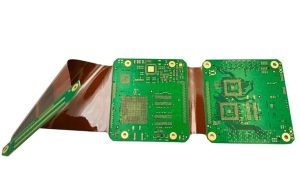
A Rigid-Flex PCB is a circuit board that combines rigid PCB sections with flexible circuit sections within a single integrated PCB structure.
The rigid portions are commonly constructed using FR-4 or other rigid laminates and provide mechanical support for components and mounting hardware. The flexible portions typically use polyimide-based dielectric materials and flexible copper to create bendable electrical connections between rigid sections.
A true rigid-flex PCB is different from a flexible PCB with an attached stiffener. A stiffener reinforces a localized area of a flexible circuit, usually to support a connector or component. In contrast, a rigid-flex PCB contains both rigid and flexible regions as part of the designed multilayer construction.
The flexible circuit extends continuously through the rigid and flexible regions, while additional rigid materials are laminated into selected areas to create mechanically stable component-mounting sections.
Rigid-flex designs commonly reference IPC standards such as IPC-2223 for flexible and rigid-flex circuit design and IPC-6013 for qualification and performance requirements. The exact standards and acceptance criteria should be selected according to the application and product requirements.
By integrating multiple circuit boards and interconnects into one structure, rigid-flex technology can reduce connector count, simplify assembly, improve packaging efficiency, and potentially reduce overall system weight and volume.
Rigid-Flex PCB Structure and Stackup Design
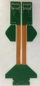
The stackup is one of the most important aspects of Rigid-Flex PCB Design. Unlike a conventional rigid PCB with a relatively uniform thickness, a rigid-flex PCB can have different layer structures and thicknesses in different regions.
The stackup determines:
- Number of copper layers
- Flexible and rigid dielectric materials
- Copper thickness
- Overall thickness
- Bend region construction
- Rigid-to-flex transition structure
- Impedance characteristics
- Mechanical flexibility
- Thermal and electrical performance
Rigid-Flex Layer Architecture
A typical rigid-flex construction uses a continuous flexible core that extends through the flexible region and, depending on the construction, may continue underneath the rigid regions.
Additional FR-4 cores and prepreg materials are laminated into the rigid sections to provide mechanical thickness and component support. Flexible copper is generally protected with a polyimide coverlay, while rigid sections commonly use solder mask.
The exact construction varies significantly according to the number of layers, bend requirements, manufacturing process, and electrical requirements.
Example Rigid-Flex PCB Stackup
| Layer | Typical Material | Region |
|---|---|---|
| Top copper | Copper foil | Rigid region |
| Rigid core | FR-4 or high-Tg laminate | Rigid region |
| Inner copper | Rolled annealed copper | Rigid + flex region |
| Flexible dielectric | Polyimide | Rigid + flex region |
| Inner copper | Rolled annealed copper | Rigid + flex region |
| Rigid core | FR-4 or high-Tg laminate | Rigid region |
| Bottom copper | Copper foil | Rigid region |
| Coverlay | Polyimide + adhesive system | Flexible region |
| Solder mask | LPI solder mask | Rigid region |
This is only a representative construction. Actual stackups should be developed together with the PCB manufacturer because lamination methods, material availability, bend requirements, impedance targets, and fabrication capabilities can substantially change the final structure.
Rigid-Flex PCB Thickness
Rigid-flex PCBs do not necessarily have one uniform thickness.
The rigid regions are typically thicker because they contain additional FR-4 or other rigid dielectric layers. The flexible region is intentionally thinner to allow bending.
Typical thickness ranges vary considerably by construction. A rigid section may be approximately 0.8–2.4 mm thick, while the flexible section may be approximately 0.1–0.4 mm thick. These values are design examples rather than universal manufacturing limits.
The thickness of the flexible section directly affects:
- Minimum bend radius
- Flexibility
- Dynamic bending life
- Mechanical stress
- Copper fatigue
- Overall packaging space
Rigid-Flex PCB Materials
Material selection is critical because the rigid and flexible regions must satisfy different mechanical and electrical requirements.
Polyimide
Polyimide is widely used as the flexible dielectric because of its flexibility, thermal stability, and electrical insulation properties.
Rolled Annealed Copper
Rolled Annealed (RA) Copper is commonly preferred for dynamic flex regions because its mechanical structure is better suited to repeated bending than conventional electrodeposited copper.
FR-4
FR-4 is commonly used in rigid sections because it provides mechanical support and is compatible with conventional PCB assembly processes.
High-Tg Materials
High-Tg laminate materials may be selected when the rigid portion must withstand elevated processing or operating temperatures.
Coverlay
A polyimide coverlay protects copper traces in flexible regions. Unlike conventional solder mask, coverlay is commonly used to provide mechanical and environmental protection while maintaining flexibility.
Types of Rigid-Flex PCBs
There is no single standard rigid-flex PCB configuration. The construction depends on circuit complexity, layer count, bending requirements, and mechanical packaging.
1. Double-Layer Rigid-Flex PCB
A simple rigid-flex design may contain two copper layers with rigid sections connected through a flexible region.
This configuration is suitable for relatively simple interconnections where space savings and mechanical flexibility are important.
2. Multilayer Rigid-Flex PCB
Multilayer rigid-flex PCBs contain multiple copper layers integrated into rigid and flexible sections.
They are suitable for more complex applications requiring:
- High routing density
- Controlled impedance
- Multiple power domains
- High-speed signal routing
- Compact three-dimensional packaging
Applications include aerospace electronics, medical imaging equipment, communication systems, and industrial electronics.
3. Double-Sided Rigid-Flex PCB
Components can be mounted on both sides of the rigid sections, increasing component density and allowing more efficient use of available space.
4. Dynamic Rigid-Flex PCB
Dynamic rigid-flex PCBs are designed for applications where the flexible section repeatedly bends during operation.
Examples include:
- Robotic joints
- Foldable electronics
- Scanning mechanisms
- Moving industrial equipment
- Certain compact electromechanical systems
Dynamic applications require significantly more attention to bend radius, copper geometry, material selection, neutral-axis design, and flex-life testing than static installation applications.
Rigid-Flex PCB Manufacturing Process
Rigid-flex manufacturing is more complex than conventional rigid PCB manufacturing because multiple materials and mechanical regions must be integrated into a single structure.
A typical PCB Manufacturing process includes the following stages.
Step 1 – Flexible Inner-Layer Fabrication
Flexible polyimide material and RA copper are prepared for circuit formation.
The copper is imaged, etched, inspected, and processed according to the circuit design.
Electrical and dimensional inspection is important because defects in the flexible inner layers can become difficult to repair after lamination.
Step 2 – Coverlay and Rigid-Layer Preparation
A polyimide coverlay is prepared for the flexible regions.
The coverlay may contain openings for pads, vias, and other required features. Rigid FR-4 cores and prepreg materials are also prepared for the rigid sections.
Accurate registration is particularly important because the transition between rigid and flexible regions must maintain both mechanical and electrical integrity.
Step 3 – Full Stackup Lamination
The flexible layers, rigid cores, prepreg, copper layers, and other materials are aligned and laminated according to the specified stackup.
This is one of the most critical stages of rigid-flex PCB Manufacturing.
Lamination parameters must be carefully controlled because excessive pressure, temperature, or material flow can affect the flexible region and rigid-to-flex transition.
Step 4 – Drilling and Copper Plating
After lamination, required holes are drilled.
Depending on the design, these may include:
- Plated through-holes
- Blind vias
- Mechanical holes
- Mounting holes
A thin electroless copper layer is deposited on hole walls, followed by electrolytic copper plating to establish reliable electrical connections.
However, via placement must be carefully controlled. Through-holes and other rigid structures should generally remain outside the active bending area unless the construction has specifically been engineered and qualified for that purpose.
Step 5 – Outer-Layer Imaging and Etching
The outer copper layers are imaged and etched to create:
- Signal traces
- Component pads
- Ground planes
- Power distribution areas
- Other copper features
Controlled registration is essential because rigid-flex PCBs contain multiple material boundaries and transition regions.
Step 6 – Solder Mask and Coverlay Finishing
Rigid areas typically receive solder mask, while flexible regions are protected using polyimide coverlay.
The coverlay protects flexible copper from:
- Mechanical damage
- Moisture
- Contamination
- Environmental exposure
- Repeated bending stress
Step 7 – Surface Finish
The exposed copper pads may receive a suitable surface finish, depending on the application.
Common options include:
- ENIG
- ENEPIG
- OSP
- HASL, where appropriate
The surface finish should be selected according to component requirements, solderability, environmental conditions, reliability expectations, and cost.
Step 8 – Routing and Profile Cutting
The completed PCB is separated into its final shape using appropriate mechanical routing, punching, laser processing, or other profiling methods.
Flexible areas require particular attention to avoid mechanical damage.
Step 9 – Electrical Testing and Inspection
Rigid-flex PCBs can undergo several inspection and testing processes, including:
- Automated Optical Inspection (AOI)
- Electrical continuity and isolation testing
- Flying-probe testing
- X-ray inspection for hidden solder joints where required
- Dimensional inspection
- Impedance testing where applicable
- Flex-life testing for dynamic applications
The exact test plan should be based on the application, reliability requirements, and customer specifications.
Advantages of Rigid-Flex PCBs
Reduced Connectors and Cables
One of the most important advantages of rigid-flex technology is the reduction of connectors, wires, and cable assemblies.
Replacing multiple interconnect components with an integrated PCB structure can reduce the number of potential connection points and simplify system architecture.
Smaller Size and Lower Weight
Rigid-flex PCBs can fold into three-dimensional configurations.
A system that previously required several rigid boards connected with cables may potentially be consolidated into a single rigid-flex structure, creating significant packaging advantages.
The actual reduction in weight and volume depends on the original architecture and should be evaluated on a system-by-system basis.
Improved Reliability
Every connector, cable, crimp, and soldered interconnect introduces potential failure mechanisms.
Rigid-flex technology can eliminate many of these discrete interconnections, reducing assembly complexity and the number of interfaces that need to be managed.
For demanding applications, however, the reliability of the flex region still depends heavily on correct materials, bend radius, copper construction, routing, and manufacturing quality.
Three-Dimensional Assembly
A major advantage of rigid-flex PCB technology is its ability to support three-dimensional packaging.
The flexible sections can be folded around mechanical structures or positioned between different mounting surfaces.
This is particularly valuable when the available internal space is irregular or highly constrained.
Simplified Final Assembly
A rigid-flex design can replace multiple boards, connectors, and cable assemblies with a more integrated structure.
This can reduce:
- Assembly steps
- Wiring operations
- Connector insertion
- Mechanical fastening
- Potential assembly errors
Improved Signal Integrity
Rigid-flex construction can provide a continuous electrical path between rigid sections without requiring additional connector transitions.
For high-speed applications, this can reduce certain impedance discontinuities associated with connectors and cable interfaces.
However, signal integrity still depends on stackup design, reference planes, trace geometry, dielectric properties, return paths, and connector transitions elsewhere in the system.
Rigid-Flex PCB Applications
Rigid-flex technology is used in applications where compact packaging, reliability, mechanical flexibility, and electrical integration are important.
Medical Electronics
Rigid-flex PCBs can be used in:
- Surgical instruments
- Endoscopic equipment
- Diagnostic equipment
- Medical imaging systems
- Portable medical devices
- Implantable electronic systems, where the complete material and device design must satisfy applicable medical requirements
For implantable products, PCB material selection alone is not sufficient to establish biocompatibility. The complete device construction, encapsulation, sterilization, and regulatory requirements must be evaluated.
Aerospace and Defense
Aerospace electronics often require compact, lightweight, vibration-resistant interconnect solutions.
Rigid-flex PCBs can be used in:
- Avionics
- Satellite electronics
- Navigation equipment
- Radar systems
- Aerospace instrumentation
- Military electronics
The actual environmental requirements should be defined according to the specific platform and applicable standards.
Consumer Electronics
Rigid-flex technology is common in compact consumer products where components must fit into irregular three-dimensional spaces.
Applications include:
- Foldable devices
- Smartphones
- Cameras
- Wearable electronics
- Laptops
- Compact electronic modules
- Drones
Industrial and Robotics
Industrial equipment and robotic systems often contain moving mechanical sections.
Rigid-flex PCBs can provide integrated electrical connections between:
- Robotic joints
- Sensors
- Actuators
- Cameras
- Control modules
- Moving mechanisms
Dynamic applications require specialized flex construction and mechanical validation.
Automotive Electronics
Rigid-flex PCBs can be used in:
- Advanced driver-assistance systems
- Infotainment systems
- Instrument clusters
- Cameras
- Sensors
- Battery electronics
- Compact control modules
Automotive designs may need to withstand vibration, thermal cycling, humidity, and long operating lifetimes. Specific temperature requirements should be established from the vehicle-level specification rather than applying one universal temperature range to all rigid-flex PCBs.
Rigid-Flex PCB Design Guidelines
Rigid-Flex PCB Design differs significantly from conventional rigid-board layout because mechanical behavior is directly connected to electrical performance.
Define Flex Areas Early
The rigid and flexible regions should be defined before detailed routing begins.
The flex boundary affects:
- Stackup
- Coverlay openings
- Stiffener locations
- Via placement
- Trace routing
- Bend radius
- Mechanical clearance
Late changes to the flex boundary can require significant PCB redesign.
Follow the Required Minimum Bend Radius
The minimum bend radius depends on:
- Flex thickness
- Number of flexible layers
- Copper thickness
- Copper type
- Static or dynamic bending
- Required flex cycles
A commonly used starting point for static bending is approximately 3× the flexible-section thickness, while dynamic applications may require substantially larger radii, often around 10× thickness or more.
These are design starting points rather than universal limits. The PCB manufacturer should validate the final bend radius against the selected materials and required flex life.
Use RA Copper for Dynamic Flex Regions
Rolled annealed copper is generally preferred for repeated bending because of its favorable ductility and fatigue characteristics.
Electrodeposited copper may be suitable for certain flex constructions, but it should not automatically be treated as interchangeable with RA copper in dynamic applications.
Route Traces Carefully Through Bend Areas
Trace routing is particularly important in the flex region.
Where practical:
- Avoid sharp trace corners
- Use smooth routing
- Avoid unnecessary copper concentration
- Maintain appropriate spacing
- Avoid abrupt changes in trace width
- Follow the manufacturer’s bend-region routing rules
Trace orientation should be determined based on the bending mode and manufacturer’s mechanical guidance rather than applying a single universal routing rule to every rigid-flex design.
Keep Rigid Features Out of Active Bend Areas
Components, stiffeners, vias, plated through-holes, and other rigid structures should normally be kept away from the active bending zone unless specifically designed and qualified for flexing.
This reduces localized mechanical stress and improves flex reliability.
Use Teardrops at Critical Transitions
Teardrops can improve the mechanical transition between traces and pads by distributing stress over a larger area.
They can be particularly useful around rigid-to-flex transition areas when permitted by the fabrication process.
Perform DFM Review Before Manufacturing
Rigid-flex PCBs are typically more expensive and less forgiving of design errors than conventional rigid PCBs.
A comprehensive DFM Review should verify:
- Bend radius
- Flex-region dimensions
- Coverlay openings
- Stiffener design
- Via locations
- Copper thickness
- Layer registration
- Material availability
- Impedance requirements
- Manufacturing tolerances
Early DFM review can prevent expensive prototype iterations and production delays.
Rigid-Flex PCB Cost Factors
Rigid-flex PCBs generally have higher fabrication costs than conventional rigid PCBs because their manufacturing process combines multiple materials, specialized lamination structures, and tighter mechanical requirements.
However, the bare PCB price does not represent the complete system cost.
Major cost factors include:
Order Volume
Prototype quantities usually have a higher unit cost because engineering, tooling, setup, and inspection expenses are distributed across fewer boards.
Higher production volumes can reduce the unit cost.
Layer Count
More copper layers increase material consumption, lamination complexity, registration requirements, and processing steps.
Via Technology
Blind and buried vias can increase manufacturing complexity, particularly when sequential lamination is required.
Number of Rigid and Flexible Regions
More complex mechanical structures require more complicated material cutouts and lamination configurations.
Board Size and Thickness
Larger boards consume more material and may require more challenging processing.
Flexible-section thickness also directly affects bending performance and manufacturing requirements.
RA Copper
RA copper is often selected for dynamic flex areas, but it can affect material cost compared with conventional copper constructions.
Surface Finish
ENIG, ENEPIG, OSP, and other finishes have different material, process, and performance characteristics.
Controlled Impedance
High-speed rigid-flex designs may require tightly controlled dielectric thickness, trace geometry, and material properties, increasing engineering and manufacturing requirements.
Lead Time
Accelerated prototype or production schedules may increase manufacturing costs because of additional scheduling and processing requirements.
When evaluating rigid-flex technology, buyers should compare the complete system cost rather than only the PCB quotation. Connector costs, cable assemblies, assembly labor, mechanical space, wiring complexity, and field-service considerations can all affect the total cost of ownership.
How to Choose a Rigid-Flex PCB Manufacturer
Not every conventional PCB manufacturer has the process capability required for reliable rigid-flex production.
When selecting a Rigid-Flex PCB Manufacturer, consider the following factors.
Verify Rigid-Flex Manufacturing Experience
Ask whether the manufacturer has experience with the specific:
- Layer count
- Flex thickness
- Bend requirements
- Copper thickness
- Material combination
- Surface finish
- Impedance requirements
Experience should be relevant to your actual construction rather than based solely on general PCB manufacturing capability.
Evaluate Material Processing Capability
The manufacturer should understand how to process polyimide, FR-4, RA copper, coverlay, stiffeners, prepreg, and other materials used in the proposed construction.
Evaluate DFM Engineering Support
A capable supplier should be able to review:
- Stackup
- Bend radius
- Flex boundaries
- Via placement
- Coverlay openings
- Stiffeners
- Mechanical dimensions
- Impedance requirements
Check Quality Management and Applicable Standards
Depending on the application, customers may require quality systems and standards such as ISO 9001, ISO 13485, AS9100, IPC-6013, or IPC-A-600/A-610.
The applicable requirements should be determined by the product, industry, and customer specification rather than assuming that every rigid-flex PCB requires every standard.
Evaluate Testing Capability
Ask whether the supplier can provide the testing required by your design, such as:
- AOI
- Electrical continuity and isolation testing
- Flying-probe testing
- X-ray inspection
- Dimensional inspection
- Impedance testing
- Flex-life testing
- Functional testing when applicable
Review Prototype Capability
Prototype capability is especially important for rigid-flex projects because the first production run may reveal mechanical issues that are difficult to identify from electrical design data alone.
A strong prototype process should allow the engineering team to validate:
- Mechanical fit
- Bend performance
- Component clearance
- Assembly process
- Electrical performance
- Flex reliability
Rigid-Flex PCB Manufacturing with Kingda
For projects requiring integrated PCB Design and PCB Manufacturing, Kingda can be considered as a manufacturing partner for rigid-flex PCB development and production.
The key point when selecting a supplier is not simply whether the company can manufacture a rigid-flex board, but whether it can support the complete engineering process from stackup development and DFM review through fabrication, inspection, and testing.
For complex rigid-flex projects, early communication between the PCB designer and manufacturer is particularly important. Mechanical drawings, bend requirements, layer stackups, material specifications, impedance requirements, component locations, and assembly requirements should be reviewed before production begins.
Conclusion
Rigid-flex PCB technology combines the component-support capability of rigid PCBs with the three-dimensional flexibility of flexible circuits.
Its primary benefits include reduced connector and cable requirements, compact packaging, simplified assembly, improved integration, and the ability to fit complex mechanical structures.
However, rigid-flex technology also requires specialized PCB Design and PCB Manufacturing expertise. Bend radius, flexible materials, RA copper, coverlay, via placement, rigid-to-flex transitions, stackup construction, and DFM requirements must all be considered during development.
For medical devices, aerospace electronics, automotive systems, robotics, cameras, and compact consumer electronics, rigid-flex PCBs can provide an effective solution when conventional rigid or flexible PCBs cannot meet the complete mechanical and electrical requirements.
The most important step is to involve an experienced manufacturer early in the design process. A well-engineered stackup and manufacturing plan can reduce prototype iterations, improve reliability, and help ensure that the final rigid-flex PCB performs as intended throughout its service life.
Article Summary
A Rigid-Flex PCB integrates rigid and flexible circuit technologies into a single PCB structure, allowing engineers to achieve compact three-dimensional packaging while reducing connectors, cables, and assembly complexity. Successful rigid-flex development requires careful PCB Design, appropriate material selection, controlled bend radius, suitable copper construction, reliable rigid-to-flex transitions, and professional PCB Manufacturing. Choosing a manufacturer with relevant rigid-flex process capabilities and strong DFM support is essential for achieving reliable production results.