Blind and Buried Vias: PCB Design, PCB Manufacturing & HDI Via Guide
As modern electronic products become smaller, thinner, and more powerful, conventional through-hole structures can consume valuable PCB routing space. To overcome this limitation, advanced multilayer boards increasingly use specialized interconnection technologies such as Blind Vias and Buried Vias.
A printed circuit board (PCB) consists of multiple copper layers separated by dielectric materials. Electrical connections between these layers are established through vias. Unlike through-hole vias, which typically extend through the entire board, blind and buried vias connect only selected layers. This makes them particularly useful for high-density interconnects, compact products, and advanced PCB Design.
This article explains what blind and buried vias are, how they differ, how they are manufactured, and where they are used. It also discusses important considerations for PCB Manufacturing, including sequential lamination, laser drilling, plating, aspect ratio, and design for manufacturability.
What Are Blind Vias and Buried Vias?
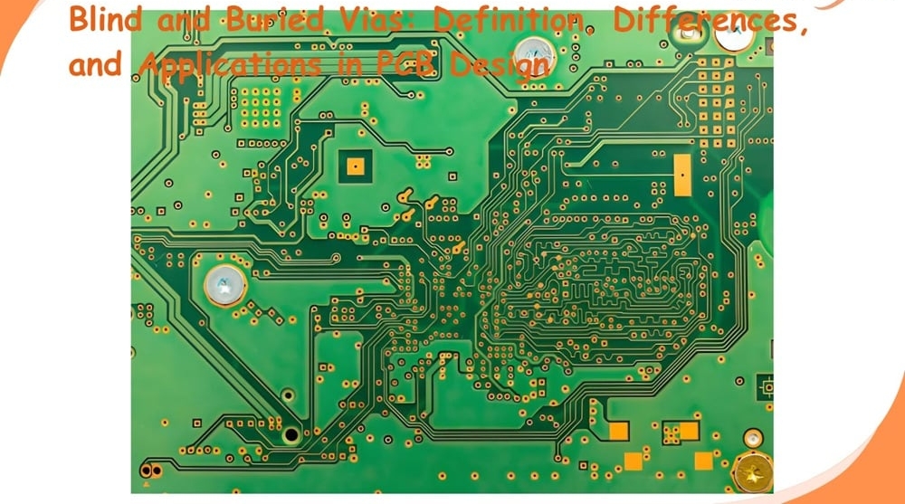
Blind vias and buried vias are specialized PCB Via structures used to create electrical connections between selected layers of a multilayer PCB.
Although both are drilled or formed within the PCB structure, their connection paths are different.
- A Blind Via connects an outer copper layer to one or more internal layers without extending completely through the PCB.
- A Buried Via connects two or more internal copper layers and does not reach either outer surface.
- A through-hole via extends through the entire PCB and can connect multiple layers along its full depth.
These structures allow engineers to use otherwise unavailable routing space, making them important technologies for HDI PCB and high-density multilayer designs.
What Is a Blind Via?
A blind via is a conductive hole that connects an outer layer of a PCB to one or more internal layers without passing completely through the board.
For example, a blind via may connect Layer 1 to Layer 2 or Layer 3 while stopping before reaching the opposite side of the board.
Because one end of the via is connected to an outer layer, its opening is accessible from the top or bottom surface of the PCB. However, the via does not pass through the entire board.
Key Characteristics of Blind Vias
- Connect an outer copper layer with one or more internal layers.
- Do not extend through the complete PCB thickness.
- Can be produced using laser drilling or controlled mechanical drilling, depending on the structure.
- Help free routing space on densely populated layers.
- Are widely used in HDI PCB designs.
- Can be used to support fine-pitch BGA and other high-density components.
- Require careful control of drilling depth, registration, plating, and aspect ratio.
Blind vias are particularly useful when the outer layer contains densely packed components and conventional through-hole vias would interfere with routing.
What Is a Buried Via?
A buried via is a conductive interconnection that connects two or more internal PCB layers without reaching either external surface.
Because both ends of the via are located inside the PCB stackup, the via cannot be seen from the top or bottom of the finished board.
For example, a buried via may connect Layer 2 to Layer 3 or Layer 3 to Layer 5 in a multilayer PCB. The exact structure depends on the layer stackup and manufacturing process.
Key Characteristics of Buried Vias
- Connect internal copper layers only.
- Do not connect directly to the top or bottom surface.
- Are manufactured within an internal PCB structure before final board lamination.
- Can increase routing flexibility in multilayer designs.
- Help reduce the number of through-hole structures required.
- Are useful for power, ground, and signal interconnections in complex multilayer boards.
- Generally require more complicated manufacturing and registration control than conventional through-hole vias.
Buried vias are particularly valuable when routing density is high and the designer needs to create connections between internal layers without consuming space on the external layers.
Blind and Buried Vias in PCB Design
Both blind and buried vias play important roles in advanced PCB Design, but their construction and application are different.
Blind Via Design
Blind vias are used when a connection is required between an external layer and selected internal layers.
A typical blind-via design process includes:
- Defining the required layer-to-layer connection.
- Selecting an appropriate via diameter and pad size.
- Determining the drilling or laser process.
- Checking the required via depth.
- Maintaining adequate annular ring and registration tolerance.
- Confirming the structure with the PCB manufacturer’s manufacturing capabilities.
For advanced HDI boards, laser-drilled microvias are frequently used because their small diameter and shallow depth allow high-density routing.
Buried Via Design
Buried vias are designed entirely within the internal layer structure.
Important design considerations include:
- Defining the exact internal layers to be connected.
- Creating appropriate drill and fabrication data for the selected construction.
- Maintaining sufficient pad and annular-ring dimensions.
- Ensuring adequate layer-to-layer registration.
- Considering the number of sequential lamination cycles.
- Confirming that the manufacturer can reliably fabricate the required buried-via structure.
Because buried vias are inaccessible after final lamination, the internal fabrication sequence must be carefully planned before manufacturing begins.
Blind Via and Buried Via Aspect Ratio
Aspect ratio is an important parameter in via design.
It is commonly expressed as:
Aspect Ratio = Via Depth ÷ Finished Hole Diameter
The acceptable aspect ratio depends on the via type, drilling technology, copper plating process, board thickness, material system, and manufacturer’s capabilities.
For laser-drilled microvias, a depth-to-diameter ratio around 1:1 or lower is commonly targeted because shallow structures are easier to drill, desmear, and plate reliably.
For mechanically drilled buried vias, the achievable aspect ratio can differ significantly from microvias. Therefore, a fixed ratio such as “1:12” should not be treated as a universal specification. Designers should instead obtain the manufacturer’s actual minimum drill size, maximum drilling depth, plating capability, and aspect-ratio limits before finalizing the stackup.
This is particularly important in high-density PCB Manufacturing, where small changes in via geometry can significantly affect yield and reliability.
Blind and Buried Via Manufacturing Process
Manufacturing blind and buried vias is more complicated than manufacturing conventional through-hole vias because the vias must terminate at specific layers.
A typical process may include the following stages.
1. Stackup Engineering
The manufacturer first defines the PCB layer structure, dielectric thickness, copper thickness, via locations, and layer-to-layer connections.
For HDI constructions, the stackup must be designed together with the via structure because via depth and dielectric thickness are closely related.
2. Inner-Layer Fabrication
For buried-via structures, the relevant internal layers are fabricated first.
The process may include:
- Copper imaging
- Etching
- Inspection
- Drilling
- Desmear
- Electroless copper deposition
- Electrolytic copper plating
The exact sequence depends on the PCB construction and fabrication technology.
3. Sequential Lamination
Sequential lamination is commonly used for advanced multilayer and HDI constructions.
Instead of manufacturing the entire board in a single lamination step, selected layers are fabricated and laminated in stages. This allows manufacturers to create buried and blind interconnections between specific layer groups.
The number of sequential lamination cycles depends on the required via structure and overall stackup.
4. Laser Drilling
Laser drilling is widely used for microvias and certain blind-via structures.
A laser removes dielectric material to expose the underlying copper target pad. The drilling depth and diameter must be tightly controlled to prevent damage to the target copper or surrounding dielectric.
Laser drilling is particularly useful for Microvias, where conventional mechanical drilling would be too large or difficult to control.
5. Mechanical Drilling
Mechanical drilling may be used for larger blind or buried vias when the board construction allows it.
For buried vias, drilling is generally performed on an internal subassembly before the final layers are laminated around it.
6. Desmear and Copper Plating
After drilling, the hole walls must be properly cleaned and prepared for metallization.
A typical process includes:
- Hole cleaning and desmear
- Surface conditioning
- Electroless copper deposition
- Electrolytic copper plating
The copper plating forms a conductive path along the via wall.
For structures requiring high reliability, the manufacturer must carefully control copper thickness, plating uniformity, voids, cracks, and interface quality.
7. Via Filling When Required
Some HDI designs use filled and capped microvias or via-in-pad structures.
Via filling can provide a flat surface for component assembly and can also allow additional routing structures to be placed over the via.
However, via filling is not automatically required for every blind or buried via. The need depends on the component pitch, pad structure, routing requirements, and manufacturing process.
8. Outer-Layer Processing
After the required internal via structures are completed, the remaining PCB layers are laminated and processed.
The manufacturer then performs:
- Outer-layer imaging
- Etching
- Solder mask application
- Surface finishing
- Silkscreen
- Routing or profiling
- Electrical testing
- Final inspection
9. Inspection and Testing
Advanced via structures require strict quality control.
Typical inspection methods may include:
- Automated Optical Inspection (AOI)
- Electrical testing
- Microsection analysis
- X-ray inspection where appropriate
- Dimensional inspection
- Plating-thickness verification
- Impedance testing for controlled-impedance designs
Microsection analysis is particularly useful for evaluating via barrel quality, copper thickness, layer registration, voids, and interconnection reliability.
Manufacturing Technologies for Blind and Buried Vias
Several technologies may be used depending on the PCB construction.
Laser Drilling
Laser drilling is one of the most common technologies for microvias and HDI blind-via structures. It provides precise control over small hole diameters and shallow depths.
Mechanical Drilling
Mechanical drilling remains important for larger blind and buried vias where the required geometry is compatible with mechanical drilling equipment.
Sequential Lamination
Sequential lamination enables manufacturers to build complex layer structures in stages. It is especially important for multilayer HDI boards with multiple via levels.
Plasma Processing
Plasma processes can be used in specialized PCB fabrication applications for dielectric treatment and hole-related processing. However, plasma etching should not be regarded as a universal replacement for laser or mechanical drilling.
Photo-Defined Via Technologies
Certain advanced PCB technologies use photolithographic or photo-defined dielectric processes to create very small interconnection structures. These are specialized processes and are generally selected according to the manufacturer’s material system and HDI technology.
Blind Vias vs. Buried Vias
| Feature | Blind Vias | Buried Vias |
|---|---|---|
| Connection | Outer layer to one or more internal layers | Internal layer to internal layer |
| Outer opening | Present on the connected outer surface | None |
| Visibility | Opening may be visible from the connected PCB surface | Completely enclosed inside the PCB |
| Typical manufacturing | Laser or controlled mechanical drilling | Internal drilling followed by lamination |
| Main purpose | Increase outer-layer routing density | Increase internal routing flexibility |
| Typical application | HDI, fine-pitch BGA, compact electronics | Complex multilayer routing |
| Manufacturing complexity | Higher than through-hole vias | Generally higher than conventional through-hole vias |
Blind and Buried Vias vs. Through-Hole Vias
Through-hole vias extend through the entire PCB thickness and can connect multiple layers along their full length.
Blind and buried vias, in contrast, connect only selected layers.
| Feature | Blind & Buried Vias | Through-Hole Vias |
|---|---|---|
| Connection | Selected layers | Typically extends through the entire board |
| Routing density | High | Lower in dense areas |
| Manufacturing complexity | Higher | Lower |
| Cost | Generally higher | Generally lower |
| Layer utilization | More flexible | Consumes routing space across layers |
| Typical applications | HDI and advanced multilayer PCB | Conventional multilayer and through-hole designs |
| Design flexibility | High | Relatively simple |
The choice between these via structures should be based on electrical, mechanical, manufacturing, and cost requirements rather than routing density alone.
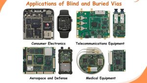
Applications of Blind and Buried Vias
Consumer Electronics
Smartphones, tablets, laptops, wearable devices, and other compact products often require extremely high routing density.
Blind vias and microvias allow designers to route connections within limited PCB space and support fine-pitch components.
Telecommunications
Networking equipment, communication modules, RF systems, and high-speed digital platforms may use advanced via structures to optimize routing and signal paths.
For high-speed designs, via geometry should be considered together with the signal return path, impedance, layer transitions, and parasitic effects.
Aerospace and Defense Electronics
Aerospace and defense electronics can require compact and highly integrated PCB assemblies.
Blind and buried vias can help reduce board size and provide greater routing flexibility, although the appropriate PCB construction depends on reliability, environmental, qualification, and application requirements.
Medical Electronics
Medical equipment such as imaging systems, diagnostic instruments, monitoring equipment, and other compact electronic systems may use high-density multilayer PCB technologies.
The specific PCB construction depends on electrical performance, reliability, thermal management, mechanical constraints, and applicable regulatory requirements.
Automotive Electronics
Advanced automotive electronics increasingly require compact and high-density circuit structures.
Blind vias and microvias can support applications such as ADAS electronics, infotainment systems, control modules, sensors, and communication systems when the required manufacturing technology is appropriate.
Advantages of Blind and Buried Vias
Higher Routing Density
Blind and buried vias allow designers to establish layer-specific connections without occupying the same routing space as a full through-hole via.
Better Space Utilization
Because the vias do not necessarily pass through the entire board, unused routing areas on certain layers can be recovered.
Support for HDI Designs
Blind vias and microvias are fundamental technologies in many HDI PCB constructions.
Greater Layout Flexibility
Designers can create more flexible connections between selected layers, which is useful for high-density component layouts.
Smaller PCB Footprint
By reducing the routing space consumed by conventional through-hole vias, advanced via structures can help engineers achieve smaller PCB designs.
Limitations of Blind and Buried Vias
The advantages of these technologies come with additional manufacturing requirements.
Higher Manufacturing Cost
Additional drilling, plating, lamination, inspection, and process-control requirements generally increase manufacturing cost.
More Complicated Fabrication
Blind and buried vias require closer coordination between PCB Design and manufacturing engineering.
Tighter Registration Requirements
As the number of layers and sequential processes increases, layer-to-layer registration becomes increasingly important.
More Difficult Inspection
Buried vias are enclosed within the PCB and cannot be visually inspected from the external surface. Cross-section analysis and other process-control methods may therefore be required.
More Demanding DFM Requirements
A design that looks electrically feasible may not necessarily be manufacturable at the desired yield. Via diameter, depth, pad size, copper thickness, dielectric thickness, and layer registration must all be reviewed during DFM.
Key PCB Design Considerations for Blind and Buried Vias
Define the Layer Stackup Early
The via structure should be considered when developing the multilayer stackup rather than being added after routing is completed.
Check Via Geometry
Verify:
- Finished hole diameter
- Pad diameter
- Via depth
- Aspect ratio
- Annular ring
- Target-pad size
- Copper thickness
Consider Signal Integrity
A via transition introduces discontinuities into high-speed signal paths.
Engineers should consider:
- Via capacitance
- Parasitic inductance
- Return-current path
- Reference-plane continuity
- Impedance discontinuity
- Stub length
Blind vias can reduce unnecessary via stubs in some designs, which can be beneficial for high-speed signaling.
Plan Thermal Paths
For power electronics and thermally demanding applications, via structures may also be part of the thermal design.
Thermal vias, copper planes, and appropriate materials should be evaluated together with the electrical design.
Follow Manufacturer Design Rules
The most important design rule is to use the actual capability of the selected PCB manufacturer.
Before finalizing a blind or buried via design, engineers should confirm:
- Minimum finished via diameter
- Maximum via depth
- Minimum pad size
- Minimum annular ring
- Available laser-drilling capability
- Mechanical drilling capability
- Sequential lamination capability
- Copper plating capability
- Via-fill capability
- Registration tolerance
- Electrical testing capability
How to Choose a Blind and Buried Via PCB Manufacturer
Selecting a suitable manufacturer is particularly important because blind and buried vias require tighter process control than conventional through-hole structures.
When evaluating a supplier, consider:
- HDI and multilayer experience – Confirm that the manufacturer routinely handles advanced multilayer and HDI structures.
- Manufacturing capability – Review laser drilling, mechanical drilling, sequential lamination, plating, and via-fill capabilities.
- DFM support – Engineering teams should review the design before production and identify manufacturability risks.
- Quality control – Ask about AOI, electrical testing, microsection analysis, plating inspection, and other relevant quality-control procedures.
- Material capability – Confirm compatibility with the required dielectric, copper weight, surface finish, and high-frequency materials.
- Prototype and production support – The manufacturer should be able to support both prototype validation and volume production when required.
- Traceability – For demanding applications, material and process traceability can be important for long-term quality management.
For projects requiring blind vias, buried vias, microvias, and complex multilayer structures, Kingda can be considered as a PCB manufacturing partner based on the project’s required specifications and validated manufacturing capabilities.
Blind and Buried Vias in Advanced PCB Manufacturing
As electronic products continue to become smaller while incorporating more functions, advanced interconnection technologies are increasingly important.
The combination of PCB Design, HDI technology, microvias, blind vias, and buried vias allows engineers to make more efficient use of limited PCB space.
However, these technologies should not be selected simply because they provide higher density. Designers should evaluate the entire system, including:
- Electrical performance
- Signal integrity
- Thermal management
- Mechanical requirements
- Manufacturing yield
- Reliability
- Testing
- Cost
- Production volume
A well-designed PCB uses the simplest viable via structure that satisfies the electrical and mechanical requirements.
Conclusion
Blind Vias and Buried Vias are important interconnection technologies for modern multilayer and HDI circuit boards. Blind vias connect an outer layer with selected internal layers, while buried vias establish connections entirely within the internal layer structure.
Compared with conventional through-hole vias, these structures provide greater routing flexibility and can improve space utilization in high-density designs. However, they also require more sophisticated manufacturing processes, including controlled drilling, sequential lamination, desmear, copper plating, registration control, and specialized inspection.
For successful PCB Manufacturing, via geometry should be considered from the earliest stage of PCB Design. Working closely with an experienced manufacturer can help ensure that the selected stackup, materials, drilling technology, plating process, and inspection methods are compatible with the required performance and production targets.
Article Summary
Blind and buried vias allow multilayer PCBs to create layer-specific electrical connections without relying exclusively on full through-hole structures. Blind vias connect external and internal layers, while buried vias connect internal layers only. They are widely used in HDI, compact electronics, telecommunications, automotive, medical, aerospace, and other advanced applications. Because they require specialized manufacturing and tighter process control, designers should verify via geometry, aspect ratio, stackup, registration, plating, and DFM requirements with the PCB manufacturer before production.