Blind and Buried Vias: PCB Design, PCB Manufacturing & Via Technology Guide
Modern PCB Design increasingly requires engineers to fit more circuitry into smaller areas. As electronic products become thinner, lighter, and more functionally integrated, conventional through-hole vias can consume valuable routing space and restrict component placement.
Blind vias and buried vias provide advanced interconnection options for multilayer and HDI circuit boards. Unlike a conventional through-hole via that passes through the entire PCB, a blind via connects an outer layer to one or more inner layers, while a buried via connects only internal layers and remains completely enclosed within the PCB structure.
These via structures can improve routing density, free up space beneath fine-pitch components, and support compact high-density interconnect designs. However, they also require more sophisticated fabrication processes, tighter manufacturing controls, and careful stackup planning.
This guide explains what blind and buried vias are, how they differ from through-hole vias, how they are designed and manufactured, and where they are commonly used.
What Are Blind and Buried Vias?
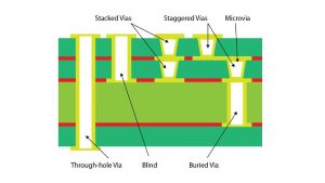
A via is a plated hole that electrically connects copper features on different layers of a PCB. Depending on where the via begins and ends, it can be classified as a through-hole via, blind via, or buried via.
What Is a Blind Via?
A blind via connects an external PCB layer to one or more internal copper layers without passing completely through the circuit board.
For example, a blind via may connect:
- Layer 1 to Layer 2
- Layer 1 to Layer 3
- Layer 6 to Layer 5
- Layer 6 to Layer 4
The via is visible or accessible from one outer surface of the PCB, but it terminates at an internal layer.
Blind vias are particularly useful when routing signals from an external component layer into dense internal routing structures.
They are widely associated with HDI PCB technology, especially when used with microvias, fine-line routing, and sequential lamination.
What Is a Buried Via?
A buried via connects two or more internal PCB layers without connecting to either outer surface.
For example, in a six-layer PCB, a buried via might connect:
Layer 2 ↔ Layer 3
or:
Layer 3 ↔ Layer 4
or:
Layer 2 ↔ Layer 5
The via is fabricated within the multilayer structure and is not visible from the top or bottom surface after the PCB is completed.
Buried vias can provide additional internal routing paths while avoiding the space occupied by through-hole vias on the outer layers.
Blind Vias vs. Buried Vias
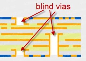
Although both are advanced via structures, their electrical connections and manufacturing processes are different.
Blind Via
A blind via:
- Starts from an outer layer
- Connects to one or more internal layers
- Does not pass through the entire board
- Is accessible from one PCB surface
- Can improve outer-layer routing density
- Is commonly used in HDI PCB structures
Buried Via
A buried via:
- Exists entirely inside the PCB
- Connects two or more internal layers
- Does not connect directly to an outer layer
- Is hidden after PCB fabrication
- Can free additional routing space on the outer layers
- Is often used in complex multilayer PCB designs
The distinction is based primarily on the via’s physical endpoints rather than simply whether the hole can be seen.
Blind and Buried Vias in PCB Design
Blind and buried vias must be considered during the initial stackup and routing stages rather than added after the PCB layout is completed.
Their use affects:
- Layer stackup
- Routing density
- Drill strategy
- Lamination sequence
- Manufacturing cost
- Impedance control
- Signal integrity
- Registration tolerance
- Via reliability
- PCB assembly clearance
Blind Via Design
Blind vias are particularly useful when a signal must move from an outer layer into an internal routing layer without consuming space on every layer between the starting and ending points.
For example:
Top Layer → Inner Layer 2
A blind via can provide this connection without extending through the lower layers.
In HDI designs, laser-drilled microvias are commonly used to create very small blind connections between adjacent layers.
Buried Via Design
Buried vias are used when a connection is required between internal layers.
For example:
Inner Layer 2 → Inner Layer 4
The via can remain completely within the multilayer structure, leaving the external layers available for component placement and routing.
This can be especially useful in dense multilayer boards where routing resources are limited.
Via Aspect Ratio
The aspect ratio of a via is an important PCB manufacturing parameter.
It is generally expressed as:
Aspect Ratio = Via Depth / Finished Hole Diameter
For example, a hole that is 0.20 mm in diameter and 0.40 mm deep has an aspect ratio of:
0.40 / 0.20 = 2:1
The achievable aspect ratio depends on the via type, drilling method, PCB material, copper plating process, board thickness, and manufacturer’s process capability.
Therefore, a fixed statement such as “blind vias always have a 1:1 aspect ratio” or “buried vias always have a 1:12 ratio” is not technically universal.
For laser-drilled microvias, the aspect ratio is generally much lower than that of conventional mechanically drilled holes. The exact design limit should be confirmed with the PCB manufacturer before layout completion.
Manufacturing Considerations for Blind and Buried Vias
Blind and buried vias require more complicated manufacturing processes than conventional through-hole vias.
The exact process depends on the PCB construction, via type, material system, and manufacturer.
Sequential Lamination
Sequential lamination is one of the most important techniques for manufacturing advanced blind and buried via structures.
Instead of laminating the entire PCB stackup in one operation, selected layers are fabricated and laminated in stages.
A simplified process may include:
- Fabricate selected inner layers.
- Drill and plate required buried vias.
- Laminate additional dielectric and copper layers.
- Form blind vias.
- Perform additional drilling and plating.
- Build the final PCB stackup.
- Complete outer-layer imaging and finishing.
- Perform electrical and dimensional inspection.
The exact sequence varies according to the stackup.
Laser Drilling
Laser drilling is widely used for small blind microvias.
Laser drilling can create precise openings in dielectric materials without requiring a conventional mechanical drill to pass through the entire board.
Common laser-drilling applications include:
- Microvias
- HDI interconnections
- Fine-pitch BGA breakout
- High-density multilayer routing
- Small blind vias
The process must be carefully controlled because dielectric thickness, copper thickness, laser parameters, target-pad size, and registration all affect the final via quality.
Mechanical Drilling
Mechanical drilling remains widely used for larger blind and buried vias, depending on the PCB construction and manufacturing process.
Drill diameter, depth control, tool wear, positional accuracy, and hole-wall quality all influence the final result.
Plasma Processing
Plasma treatment may be used in specialized PCB manufacturing processes to remove or modify dielectric material and improve surface preparation.
However, plasma etching is not a universal replacement for mechanical or laser drilling. The appropriate process depends on the material system and manufacturing technology.
Plating
After a via is formed, copper plating is required to establish electrical continuity between the connected copper layers.
Reliable plating requires good control of:
- Hole cleanliness
- Desmear
- Chemical preparation
- Copper deposition
- Plating thickness
- Current density
- Uniformity
Poor plating can result in increased resistance, discontinuities, or reliability failures.
Blind and Buried Via Manufacturing Flow
A simplified advanced via manufacturing process can be described as:
Material Preparation → Inner-Layer Fabrication → Drilling → Desmear → Copper Plating → Sequential Lamination → Blind Via Formation → Outer-Layer Fabrication → Surface Finish → Inspection → Electrical Testing
Not every blind-and-buried-via PCB follows exactly this sequence. The manufacturing flow depends on whether the board uses mechanical blind vias, laser microvias, buried vias, stacked microvias, staggered microvias, or other HDI structures.
Blind and Buried Vias in HDI PCB Design
Blind vias are strongly associated with HDI PCB technology because they allow engineers to create dense interconnections without dedicating large through-hole structures to every layer.
A conventional through-hole via can occupy routing space on multiple layers. In contrast, a blind or microvia can terminate at a selected internal layer.
This can improve:
- Routing density
- BGA breakout
- Component placement flexibility
- Board miniaturization
- Signal routing efficiency
Microvias and Blind Vias
A microvia is generally a very small via, commonly formed using laser drilling, and is typically used to connect adjacent or nearby layers in HDI structures.
Therefore:
Not every blind via is necessarily a microvia, and not every microvia is described simply as a conventional blind via.
This distinction is important when discussing advanced PCB Design.
Applications of Blind and Buried Vias
Blind and buried vias are used in applications where routing density, miniaturization, or electrical performance justifies their additional manufacturing complexity.
Consumer Electronics
Smartphones, tablets, wearable devices, compact computers, cameras, and other miniaturized products can use HDI and microvia technologies to fit complex circuitry into limited space.
Blind vias can provide efficient connections beneath fine-pitch packages and between dense routing layers.
Telecommunications Equipment
High-speed networking and telecommunications equipment often requires multilayer boards with controlled impedance, dense routing, and carefully managed signal-return paths.
Blind and buried vias can help engineers optimize routing around high-pin-count packages and dense signal interfaces.
Aerospace and Defense Electronics
Avionics and defense electronics may require compact, reliable, high-density interconnect structures.
Depending on system requirements, blind and buried vias can help reduce board size while providing complex multilayer interconnections.
Medical Electronics
Medical equipment frequently requires compact electronics combined with high reliability.
Blind and buried vias may be used in selected high-density PCB applications such as imaging equipment, monitoring systems, portable diagnostic equipment, and other sophisticated electronic assemblies.
Automotive Electronics
Advanced automotive control systems, sensors, communication modules, ADAS electronics, and other compact electronic assemblies may use HDI technologies where routing density and space constraints justify them.
Blind and Buried Vias vs. Through-Hole Vias
| Feature | Blind Via | Buried Via | Through-Hole Via |
|---|---|---|---|
| Outer-layer connection | Yes | No | Yes |
| Internal-layer connection | Yes | Yes | Yes |
| Passes through entire PCB | No | No | Yes |
| Visible from PCB surface | Accessible from one side | No | Yes |
| Manufacturing complexity | High | High | Lower |
| Typical cost | Higher | Higher | Lower |
| Routing density | High | High | Lower |
| Common applications | HDI, dense multilayer PCBs | Complex multilayer PCBs | General PCB designs |
| Common drilling method | Mechanical or laser | Mechanical or specialized process | Mechanical |
| Stackup impact | Significant | Significant | Relatively simple |
Blind and Buried Vias vs. Through-Hole Vias: Space Utilization
One of the biggest advantages of blind and buried vias is the ability to use PCB routing space more efficiently.
A conventional through-hole via extends through the entire PCB. Although the via may only connect two specific layers electrically, its physical structure occupies space on intermediate layers.
Blind and buried vias allow designers to create more localized interconnections.
For example:
Through-Hole Via
Top → Inner 2 → Inner 3 → Inner 4 → Bottom
Blind Via
Top → Inner 2
Buried Via
Inner 2 → Inner 4
This flexibility can be particularly valuable in high-density BGA fanout and HDI layouts.
Signal Integrity Considerations
Via structures can influence signal integrity, particularly in high-speed PCB designs.
Important factors include:
- Via geometry
- Via stub length
- Pad diameter
- Antipad dimensions
- Layer transition
- Reference-plane continuity
- Return-current path
- Differential-pair routing
- Impedance discontinuity
A blind via can reduce unnecessary via depth and therefore reduce the length of an unwanted via stub.
However, using blind or buried vias does not automatically guarantee better signal integrity. The entire interconnect structure must be designed and simulated appropriately.
For high-speed PCB Design, engineers should consider via transitions together with controlled impedance, reference planes, return paths, and package breakout structures.
Thermal and Reliability Considerations
Although blind and buried vias can improve routing density, they also introduce additional manufacturing variables.
Engineers should consider:
- Copper plating quality
- Thermal expansion
- Via-to-pad geometry
- Registration tolerance
- Resin and dielectric properties
- Lamination pressure
- Drill accuracy
- Copper thickness
- Thermal cycling
- Mechanical stress
For applications exposed to significant thermal cycling or mechanical stress, the via structure must be qualified against the expected operating environment.
Advantages of Blind and Buried Vias
Higher Routing Density
Blind and buried vias allow connections to be made only where required, freeing routing space on other layers.
Smaller PCB Size
More efficient routing can allow designers to reduce PCB dimensions when other design constraints permit.
Improved BGA Fanout
Blind microvias can help route fine-pitch BGA packages by providing compact connections between package pads and internal routing layers.
Better Layer Utilization
Buried vias allow internal layers to communicate without consuming space on the outer layers.
Reduced Via Stubs
Selected blind-via structures can reduce unnecessary via length, which can be beneficial for high-speed signals.
Greater Layout Flexibility
Advanced via structures give engineers more options when optimizing complex multilayer designs.
Disadvantages of Blind and Buried Vias
Higher Manufacturing Cost
The additional drilling, plating, registration, and lamination processes increase manufacturing complexity and cost.
More Complicated PCB Design
Stackup planning and via structures must be carefully coordinated.
Longer Manufacturing Cycle
Sequential processing can increase fabrication lead time compared with a simple through-hole PCB.
Tighter Manufacturing Tolerances
Blind and buried structures require better control of registration, drilling, plating, and lamination.
More Difficult Inspection
Because buried structures cannot be visually inspected from the outside, manufacturers must rely on process control, cross-section analysis, electrical testing, and other inspection methods.
Blind and Buried Via Design Guidelines
Before using blind or buried vias, PCB designers should consider the following recommendations.
Define the Stackup Early
The via structure depends directly on the layer stackup. Define the stackup before detailed routing.
Confirm Manufacturer Capabilities
Check the manufacturer’s minimum drill diameter, aspect-ratio limits, laser-via capability, copper plating capability, registration tolerance, and sequential-lamination process.
Avoid Unnecessary Complexity
Blind and buried vias should be used when their benefits justify their additional manufacturing complexity.
Optimize BGA Fanout
Use microvias and blind vias strategically around fine-pitch BGA packages rather than applying advanced vias indiscriminately.
Consider Impedance
For high-speed signals, evaluate via transitions as part of the complete controlled-impedance structure.
Consider Thermal and Mechanical Reliability
Ensure that the selected via structure is compatible with the expected temperature range, board thickness, material system, and assembly process.
Follow DFM Guidelines
A design that looks feasible in CAD may still be difficult or expensive to manufacture. Early DFM review can identify problematic via structures before fabrication.
Blind and Buried Vias in PCB Manufacturing
The success of a blind-and-buried-via PCB depends heavily on manufacturing process control.
A professional PCB Manufacturing process may include:
- Stackup verification
- Inner-layer imaging
- Etching
- Inner-layer AOI
- Mechanical or laser drilling
- Desmear
- Electroless copper
- Electrolytic copper plating
- Sequential lamination
- Outer-layer imaging
- Solder mask
- Surface finish
- Electrical testing
- Dimensional inspection
- Cross-section analysis where required
For advanced HDI boards, additional process controls may be required depending on the microvia structure and reliability requirements.
How to Choose a Blind and Buried Via PCB Manufacturer
Selecting a manufacturer is especially important because not every PCB supplier has the same HDI and sequential-lamination capabilities.
When evaluating a supplier, consider:
Engineering Capability
The manufacturer should be able to review stackups, via structures, drill files, fabrication drawings, and DFM requirements.
HDI Manufacturing Capability
Check whether the manufacturer has experience with:
- Laser microvias
- Blind vias
- Buried vias
- Sequential lamination
- Fine-line routing
- Fine-pitch BGA
- Controlled impedance
Quality Control
Ask about relevant inspection and testing capabilities, including:
- AOI
- Electrical testing
- X-ray inspection where appropriate
- Microsection analysis
- Impedance testing
- Dimensional inspection
Material Compatibility
The manufacturer should understand the selected laminate system, copper thickness, dielectric thickness, and thermal requirements.
Prototype and Mass Production
A capable supplier should be able to support both prototype validation and volume PCB Manufacturing, depending on the project requirements.
Blind and Buried Via PCB Solutions from Kingda
For complex multilayer and HDI PCB projects, Kingda can be positioned as a manufacturing partner for designs requiring advanced via structures.
A successful blind-and-buried-via project should begin with an engineering review of the PCB stackup, via structure, drill specifications, material selection, routing density, and manufacturing tolerances.
Rather than adding blind or buried vias simply because they are technically available, designers should use them where they provide a measurable benefit in routing density, miniaturization, electrical performance, or system integration.
Early communication between the PCB designer and manufacturer can also help identify manufacturability issues before fabrication begins.
Conclusion
Blind and buried vias are important technologies for modern high-density multilayer PCBs. A blind via connects an outer layer to one or more internal layers, while a buried via connects internal layers without reaching the PCB surface.
Compared with conventional through-hole vias, these structures can provide better routing efficiency, greater layer utilization, improved BGA fanout, and more compact PCB layouts. They are particularly valuable in HDI, high-density, and miniaturized electronic products.
However, blind and buried vias also require more sophisticated PCB Manufacturing processes, including specialized drilling, plating, registration control, and, in many constructions, sequential lamination. Their design should therefore be developed together with the PCB stackup and manufacturer’s process capabilities.
For engineers working on advanced PCB Design, the key is not simply to use the most advanced via technology, but to select the via structure that provides the required electrical and mechanical performance while maintaining manufacturability, reliability, and cost control.
Article Summary
Blind and buried vias are advanced PCB interconnection structures used primarily in multilayer and HDI circuit boards. Blind vias connect an outer layer with one or more internal layers, while buried vias connect only internal layers. They improve routing density and can support smaller, more complex PCB designs, but they require tighter manufacturing controls and more sophisticated processes than conventional through-hole vias. Proper stackup planning, aspect-ratio control, drilling, plating, sequential lamination, DFM review, and manufacturer capability are essential for successful blind-and-buried-via PCB production.