How to Create Gerber Files: PCB Design, PCB Manufacturing & Gerber File Guide
When you have completed a PCB Design, you cannot usually send the native CAD project directly to a PCB manufacturer and expect production to begin. Manufacturers typically need a set of standardized manufacturing files, most importantly Gerber files, together with drill data and other fabrication documentation.
Gerber files provide a graphical description of the different layers of a printed circuit board. They tell the manufacturer where copper features, solder mask openings, silkscreen graphics, and other board features should be fabricated. Drill files, typically generated in Excellon format, provide the information needed to manufacture holes and vias.
For beginners, learning how to create Gerber files may initially seem complicated. However, once the basic workflow is understood, the process is relatively straightforward. This guide explains how to generate, configure, verify, and package Gerber files for PCB Manufacturing.
What Are Gerber Files?
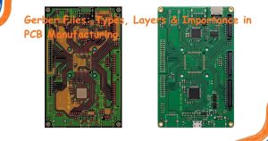
Gerber files are standardized manufacturing data files used to represent the graphical information required to fabricate a PCB. Each file normally represents one physical layer or manufacturing feature of the board.
Instead of containing the complete editable PCB design, Gerber files describe the artwork that a manufacturer needs to reproduce specific board features.
A typical PCB project may contain Gerber files for:
- Top copper
- Bottom copper
- Internal copper layers for multilayer PCBs
- Top solder mask
- Bottom solder mask
- Top silkscreen
- Bottom silkscreen
- Additional fabrication layers when required
Drill information is normally provided separately, often in Excellon drill format, rather than as a conventional Gerber artwork layer.
For engineers, PCB designers, electronics manufacturers, and hobbyists, understanding how to generate accurate Gerber files is an important part of the transition from digital PCB Design to physical PCB Manufacturing.
Why Are Gerber Files Important?
You may wonder why a manufacturer cannot simply use the original PCB design file.
The main reason is compatibility.
Different PCB CAD platforms use their own native project and database formats. For example, KiCad, Altium Designer, Autodesk Fusion Electronics/EAGLE, and other design tools may structure their source files differently. A manufacturer cannot reasonably be expected to support every native CAD format.
Gerber provides a widely adopted manufacturing data format that allows the fabrication system to interpret the required artwork independently of the designer’s original CAD software.
This makes Gerber files an important communication interface between PCB designers and manufacturers.
A properly generated Gerber package allows a manufacturer to determine:
- Where copper should be fabricated
- Where solder mask should be applied or opened
- Where silkscreen markings should appear
- Which board layers are required
- Where additional fabrication features are located
However, Gerber files do not necessarily contain every piece of information required for manufacturing. Depending on the project and manufacturer, additional files may be required for board outline, drill information, stackup, impedance requirements, fabrication notes, and other specifications.
Step-by-Step Guide: How to Create Gerber Files for a PCB
1. Finalize Your PCB Design
Before exporting manufacturing data, carefully review the PCB layout.
Generating Gerber files from an unfinished or incorrectly configured design can result in manufacturing problems that may not become obvious until the boards are fabricated.
Before exporting, check the following:
- Electrical rule check (ERC) and design rule check (DRC) results
- Trace widths and clearances
- Copper-to-board-edge clearances
- Pad and via dimensions
- Component footprints
- Drill sizes
- Board outline
- Silkscreen placement
- Reference designators
- Solder mask openings
- Copper pours and filled zones
- Layer stackup
- Controlled-impedance requirements, when applicable
It is particularly important to verify the board outline because manufacturers use this information to determine the final board dimensions and routing requirements.
If the design contains copper pours, make sure they have been properly filled or regenerated before exporting the manufacturing data.
2. Open the Gerber Export Tool
Most PCB design software provides a dedicated manufacturing-output or Gerber-generation function.
The exact menu location depends on the software version, but the workflow is generally similar.
For example:
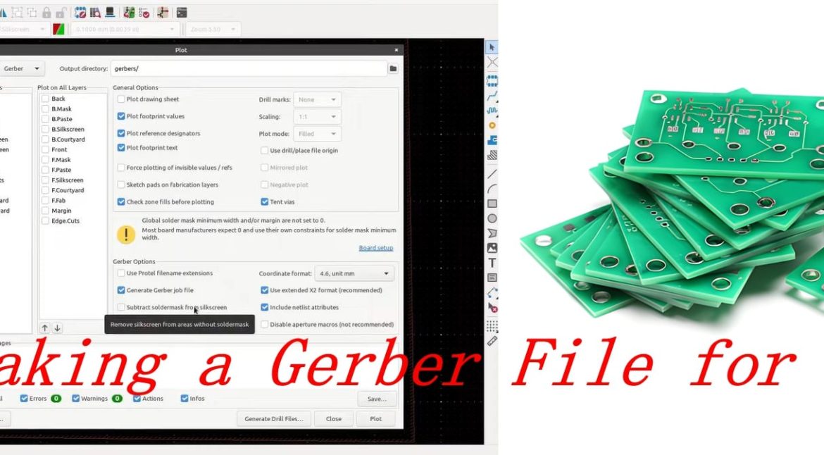
- KiCad: Plot or Gerber plotting functions in the PCB Editor
- Altium Designer: Fabrication Outputs → Gerber Files
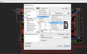
- EAGLE/Fusion Electronics: CAM Processor or manufacturing-output functions
Once the Gerber export interface is opened, you can select the layers and manufacturing data that need to be generated.
The exact options vary between CAD platforms, so always check the documentation for the software version you are using.
3. Select the Required PCB Layers
For a basic two-layer PCB, the manufacturing package commonly includes:
- Top copper
- Bottom copper
- Top solder mask
- Bottom solder mask
- Top silkscreen
- Bottom silkscreen
- Board outline or profile data
- Drill data
For a multilayer PCB, additional internal copper layers must be exported.
For example, a four-layer PCB may require:
- Top copper
- Inner copper layer 1
- Inner copper layer 2
- Bottom copper
- Top solder mask
- Bottom solder mask
- Top silkscreen
- Bottom silkscreen
- Drill data
- Board outline/profile
The exact file set depends on the board design and the manufacturer’s fabrication requirements.
Do not simply export every available CAD layer without understanding its purpose. Unnecessary or incorrectly mapped layers can create confusion during manufacturing.
4. Use Clear File Naming and Extensions
Consistent file naming makes the manufacturing package easier to interpret.
Common Gerber extensions include:
| File Extension | Typical Function |
|---|---|
.GTL |
Gerber Top Layer / Top Copper |
.GBL |
Gerber Bottom Layer / Bottom Copper |
.GTS |
Gerber Top Solder Mask |
.GBS |
Gerber Bottom Solder Mask |
.GTO |
Gerber Top Silkscreen |
.GBO |
Gerber Bottom Silkscreen |
.G1, .G2, etc. |
Internal copper layers, depending on the CAD system |
.DRL / .TXT |
Drill data, commonly Excellon |
These extensions are widely encountered, but file extensions are not the only way to identify a layer. Modern Gerber files can contain embedded attributes and metadata, and manufacturers should interpret the actual file contents rather than relying solely on filenames.
Therefore, use clear names whenever possible, such as:
Project_TopCopper.gtl
Project_BottomCopper.gbl
Project_TopMask.gts
Project_TopSilkscreen.gto
Project_Drill.drl
Clear naming reduces the possibility of layer confusion during PCB Manufacturing.
5. Configure the Gerber Output Parameters
When learning how to create Gerber files, output settings deserve particular attention.
Common parameters include:
Units
Gerber data can be generated using metric or imperial units.
Either can be used, provided the output is interpreted correctly by the manufacturer. The important point is to maintain consistency and verify the manufacturer’s requirements.
Coordinate Format
Modern Gerber workflows generally use sufficient coordinate precision for PCB fabrication.
Do not blindly choose a particular coordinate format simply because it is common in an older tutorial. The appropriate format depends on the CAD tool, Gerber version, and manufacturing workflow.
Zero Suppression
Older Gerber workflows may use different coordinate representations and zero-suppression conventions. Modern Gerber X2 workflows can include metadata that reduces ambiguity.
The safest approach is to use the manufacturer’s recommended output settings rather than assuming one universal configuration.
Gerber Format
Modern PCB manufacturing commonly uses Gerber RS-274X, while Gerber X2 adds metadata and attributes that can improve layer identification and manufacturing interpretation.
If your manufacturer specifies a particular Gerber format, follow that requirement.
6. Generate the Drill Files
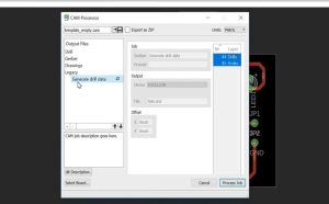
Gerber files primarily describe graphical artwork. Hole information is normally supplied separately.
Most PCB CAD tools can generate drill files, commonly in Excellon format.
Drill data can define:
- Hole locations
- Hole diameters
- Plated and non-plated hole information, depending on the output workflow
- Tool sizes
- Drill coordinates
- Drill-related manufacturing information
Drill data is essential because plated through-holes, vias, mounting holes, and other drilled features must be manufactured according to their specified dimensions and locations.
For complex boards, always verify that the drill output correctly corresponds to the PCB design and manufacturer’s requirements.
7. Include the Board Outline
The board outline is one of the most important parts of the manufacturing package.
A manufacturer needs to know the exact physical shape and dimensions of the PCB.
Depending on the CAD system, the board profile may be exported as a dedicated mechanical/profile layer or included within another manufacturing layer.
The outline should clearly define:
- Overall board dimensions
- Board shape
- Cutouts
- Slots
- Internal openings
- Rounded corners
- Routing features
For unusual mechanical shapes, make sure the manufacturer understands which geometry represents the finished board profile and which geometry is only construction information.
8. Verify the Gerber Files Using a Gerber Viewer
Do not immediately send the generated files to the manufacturer.
One of the most important steps in PCB Design and PCB Manufacturing preparation is independent verification.
Open the exported files in a Gerber viewer and inspect every layer.
Check whether:
- Copper traces appear correctly
- Pads are in the correct locations
- Vias align with the corresponding pads
- Drill holes match the intended locations
- Solder mask openings are correct
- Silkscreen text is readable
- Reference designators are not unnecessarily placed over pads
- The board outline is complete
- Internal layers are correctly identified
- Polarity and layer orientation are correct
- No unexpected artwork is present
It is especially useful to compare the Gerber viewer output against the original PCB CAD layout.
A small layer-export error can potentially result in a board that looks correct in the CAD environment but is manufactured incorrectly.
9. Check the Manufacturing Data Against the Original Design
Gerber verification should not be limited to simply checking whether the files open.
Perform a design-to-output comparison.
For example, verify that:
PCB CAD layout → Gerber copper
PCB pad/via information → Drill data
Solder mask settings → Solder mask Gerber
Silkscreen information → Silkscreen Gerber
Mechanical outline → Board profile
This cross-check helps identify missing layers, incorrect polarity, mismatched drill data, and accidental changes introduced during export.
For high-density or high-speed PCBs, additional review may be necessary for impedance-controlled traces, differential pairs, critical clearances, and other fabrication constraints.
10. Package the Manufacturing Files
After verification, place the required manufacturing files into a single folder.
Depending on the manufacturer’s requirements, the package may contain:
- Gerber files
- Excellon drill files
- Board outline/profile
- Fabrication drawing
- Stackup information
- Readme or fabrication notes
- Impedance requirements
- Special processing instructions
Compress the package into a ZIP file if requested by the manufacturer.
Before uploading, open the ZIP file and perform one final check to make sure all required files are present.
Common Gerber File Set for a Two-Layer PCB
A basic two-layer PCB may contain the following manufacturing data:
| Manufacturing Data | Purpose |
|---|---|
| Top Copper | Defines conductive features on the top layer |
| Bottom Copper | Defines conductive features on the bottom layer |
| Top Solder Mask | Defines top-side solder mask openings |
| Bottom Solder Mask | Defines bottom-side solder mask openings |
| Top Silkscreen | Defines top-side reference markings and graphics |
| Bottom Silkscreen | Defines bottom-side markings and graphics |
| Drill File | Defines hole locations and sizes |
| Board Outline | Defines the finished PCB profile |
Therefore, saying that a two-layer PCB always requires exactly a specific number of Gerber files can be misleading. The actual file count depends on the design, CAD software, manufacturing process, and additional fabrication requirements.
Common Mistakes When Creating Gerber Files
Even experienced designers can encounter manufacturing problems if the output package is not checked carefully.
Missing Internal Layers
For multilayer PCBs, forgetting to export an internal copper layer can result in incomplete manufacturing data.
Incorrect Board Outline
An incorrect or ambiguous board outline can cause problems with routing, panelization, or final board dimensions.
Missing Drill Data
Gerber artwork alone does not provide sufficient information for manufacturing drilled holes. Always include the required drill files.
Incorrect Layer Mapping
A file accidentally assigned to the wrong physical layer can result in serious fabrication errors.
Unreadable Silkscreen
Very small text or silkscreen graphics placed too close to pads may be clipped or removed during manufacturing.
Unverified Copper Pours
If copper zones are not properly regenerated before export, the Gerber output may not reflect the intended copper distribution.
Sending Only Native CAD Files
Native CAD files are useful during engineering collaboration, but they should not automatically be treated as a substitute for the manufacturer’s requested fabrication data.
If a manufacturer specifically requests Gerber and drill files, provide those files according to the manufacturer’s requirements.
Gerber Files vs Native PCB CAD Files
| Feature | Gerber Files | Native CAD Files |
|---|---|---|
| Primary purpose | Manufacturing output | Design and editing |
| Editable PCB design | No | Yes |
| Software dependency | Relatively low | High |
| Layer-based manufacturing data | Yes | Yes, but within CAD database |
| Used for fabrication | Commonly | Depends on manufacturer |
| Suitable for design modification | No | Yes |
| Manufacturing interpretation | Direct | Requires compatible CAD software |
The two file types serve different purposes.
The native CAD project is the source design environment, while Gerber files are manufacturing outputs derived from that design.
Best Practices for Reliable Gerber Generation
To improve manufacturing reliability, follow these practices:
- Complete the PCB design before generating production files.
- Run DRC and resolve relevant errors.
- Confirm the board outline and dimensions.
- Verify all copper layers.
- Verify solder mask and silkscreen layers.
- Generate and inspect drill data.
- Use the manufacturer’s preferred Gerber format and settings.
- Review the files in a Gerber viewer.
- Compare the exported data with the original PCB layout.
- Include fabrication drawings or special instructions when necessary.
- Use clear and consistent file names.
- Package all required manufacturing data together.
For advanced PCB projects, it is also good practice to confirm the stackup, copper thickness, surface finish, impedance requirements, material requirements, and other fabrication specifications before releasing the files.
Can Manufacturers Accept Native CAD Files Instead of Gerber Files?
Some PCB manufacturers and engineering service providers may accept native CAD files, particularly when they have compatible software or use automated CAD-data conversion workflows.
However, this does not mean that native CAD files should always replace Gerber data.
Gerber remains a widely used manufacturing data format, while the exact file requirements depend on the manufacturer’s process.
Before submitting a production package, ask the manufacturer which formats they accept and which additional documents are required.
Conclusion
Learning how to create Gerber files is an essential skill for anyone involved in PCB Design and PCB Manufacturing.
The basic workflow is straightforward: finalize the PCB layout, select the required manufacturing layers, configure the output settings, generate Gerber and drill files, verify the results with a Gerber viewer, and package the manufacturing data according to the manufacturer’s requirements.
The most important point is not simply generating the files—it is verifying that the exported manufacturing data accurately represents the intended PCB design.
At Kingda, we support customers with PCB manufacturing and assembly requirements, helping transform verified design data into production-ready printed circuit boards. Working with an experienced manufacturing partner can also help identify potential DFM issues before production begins.
Frequently Asked Questions
What software can generate Gerber files?
Most professional PCB design platforms can generate Gerber manufacturing data. Common examples include KiCad, Altium Designer, Autodesk Fusion Electronics/EAGLE, and other PCB CAD tools.
How many Gerber files does a simple two-layer PCB need?
A typical two-layer PCB requires top and bottom copper, top and bottom solder mask, and any required silkscreen layers, plus drill data and board-profile information. The exact number of files varies according to the CAD system and manufacturer’s requirements.
Are Gerber files the same as PCB design files?
No. Native PCB design files contain the editable design database, while Gerber files are manufacturing outputs representing individual PCB layers or features.
Do I need a drill file in addition to Gerber files?
Yes, in most standard PCB fabrication workflows. Drill data is normally provided separately, often in Excellon format, because Gerber artwork and drill information serve different manufacturing purposes.
Should I check Gerber files before sending them to a manufacturer?
Absolutely. A Gerber viewer can help you identify missing layers, incorrect artwork, misplaced silkscreen, board-outline problems, and other export issues before production.
Can Gerber files be edited like PCB CAD files?
No. Gerber files are primarily manufacturing artwork and are not intended to replace the editable source PCB design. If substantial design changes are required, it is generally better to modify the original CAD project and regenerate the manufacturing files.