Double-Sided PCB: PCB Design, PCB Manufacturing & Double-Layer PCB Guide
Printed circuit boards (PCBs) are at the heart of almost every modern electronic device, from smartphones and consumer electronics to aerospace systems and industrial control equipment. A single-sided PCB can be an economical solution for relatively simple circuits, but its limited routing capacity becomes a major constraint as circuit complexity increases.
This is where the double-sided PCB becomes valuable.
By providing copper circuitry on both sides of the board, a double-sided PCB gives engineers significantly more routing flexibility without requiring the additional fabrication complexity of a multilayer PCB. Understanding how to use a double-sided PCB effectively can help engineers and electronics designers create more compact, reliable, and cost-effective products.
What Is a Double-Sided PCB?
A double-sided PCB, also called a double-layer PCB, is a printed circuit board with conductive copper circuitry on both sides of the insulating substrate.
Unlike a single-sided PCB, which has conductive circuitry primarily on one side, a double-sided PCB provides two copper layers that can both be used for routing and component connections.
The two copper layers are electrically interconnected through plated holes, including through-hole vias and plated through-holes (PTHs). These structures allow electrical signals and power to transition between the top and bottom copper layers.
A typical double-sided PCB consists of:
- Two conductive copper layers
- An insulating substrate, such as FR-4
- Solder mask
- Silkscreen
- Plated through-holes and/or vias
- Surface-finish layers on exposed copper
The ability to route signals on both sides substantially increases the available routing area compared with a single-sided PCB.
Why Use a Double-Sided PCB?
A double-sided PCB can provide an effective balance between circuit density, performance, manufacturing complexity, and cost.
1. Higher Circuit Density
Some circuits simply cannot be routed efficiently on a single copper layer. Adding a second routing layer provides additional space for traces, power distribution, and component connections.
2. More Compact Board Size
Using both sides of the PCB can allow designers to reduce board dimensions without immediately moving to a multilayer construction.
This is particularly useful when product enclosure space is limited.
3. Greater Routing Flexibility
Two copper layers allow designers to change signal paths between the top and bottom surfaces using vias.
This can make routing complex circuits considerably easier.
4. Better Electrical Performance
A carefully planned two-layer layout can improve signal routing, power distribution, and grounding.
However, a double-sided PCB does not automatically provide better signal integrity. Performance depends on stackup, trace geometry, return-current paths, grounding strategy, component placement, and operating frequency.
5. Lower Cost Than Many Multilayer Designs
For applications that can be routed successfully using only two copper layers, a double-sided PCB can offer a simpler and potentially more economical alternative to a multilayer PCB.
It therefore occupies an important position between single-sided and multilayer circuit boards.
Double-Sided PCB Materials and Structure
Understanding the materials used in a double-sided PCB is essential for both PCB Design and PCB Manufacturing.
Substrate
The substrate provides the mechanical structure and electrical insulation between the two copper layers.
Common materials include:
- FR-4
- CEM-1
- High-Tg laminates
- Other application-specific PCB materials
FR-4 is one of the most widely used materials for general-purpose double-sided PCBs because it provides a useful combination of mechanical strength, electrical insulation, thermal performance, and cost.
Copper Layers
Copper foil is laminated to both sides of the insulating substrate.
These copper layers form:
- Signal traces
- Power connections
- Ground areas
- Component pads
- Via structures
Copper thickness is selected according to electrical, thermal, mechanical, and manufacturing requirements.
Solder Mask
The solder mask covers most exposed copper areas and helps protect the circuit from oxidation, contamination, and accidental solder bridging.
Openings are provided where soldering or electrical contact is required.
Silkscreen
The silkscreen provides reference designators, polarity indicators, logos, component labels, and other manufacturing or assembly information.
Vias and Plated Through-Holes
Vias provide electrical connections between the top and bottom copper layers.
A plated through-hole can also connect the two copper layers while providing a mounting hole for a through-hole component.
These structures are fundamental to two-layer PCB routing.
How to Use a Double-Sided PCB in PCB Design
Using both sides effectively requires careful planning during the PCB Design stage.
1. Plan Layer Usage
Unlike a multilayer PCB, a two-layer board has limited routing resources. Engineers should therefore determine how each layer will be used before detailed routing begins.
A common approach is:
- Top layer: component placement and important signal routing
- Bottom layer: additional signal routing, power distribution, ground areas, or component placement
However, there is no universal requirement that the bottom layer must be dedicated to power or ground. The optimal layer strategy depends on circuit complexity and electrical requirements.
For higher-speed designs, maintaining a continuous return-current path is often more important than simply assigning one layer to ground.
2. Optimize Component Placement
Component placement has a major impact on routing efficiency.
Large components such as:
- Microcontrollers
- Connectors
- Relays
- Transformers
- Power devices
should be positioned according to electrical, thermal, mechanical, and assembly requirements.
Smaller components can then be placed around the primary components to minimize trace length and simplify routing.
Engineers should also consider whether components are:
- Through-hole
- Top-side SMD
- Bottom-side SMD
This directly affects assembly strategy and available routing space.
3. Plan Signal Routing
Signal routing should be organized according to electrical priority.
For critical signals:
- Keep traces as short as practical.
- Avoid unnecessary vias.
- Minimize sharp geometry changes.
- Maintain appropriate return-current paths.
- Keep sensitive signals away from noisy power circuitry.
Less critical signals can generally tolerate longer routing paths.
4. Use Vias Strategically
Vias allow signals to move between the top and bottom layers.
However, excessive vias can increase routing complexity and consume valuable PCB area.
When placing vias, engineers should consider:
- Via diameter
- Drill size
- Annular ring
- Clearance
- Current capacity
- Signal integrity
- Manufacturing capability
For high-current connections, multiple vias may be used in parallel to reduce resistance and improve current distribution.
5. Plan Grounding and Power Distribution
Grounding is particularly important on a two-layer PCB because there are fewer dedicated layers available than in a multilayer board.
Where practical, designers can use large copper areas or ground pours to improve grounding and reduce impedance.
Power traces should be sized according to current requirements and allowable temperature rise.
A well-planned grounding strategy can also help reduce electromagnetic interference and improve signal integrity.
Double-Sided PCB Component Placement
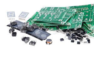
Components can be mounted on either or both sides of a double-sided PCB, depending on the design and assembly process.
Top-Side Assembly
Many products place most components on the top side to simplify inspection, assembly, and servicing.
This approach is especially common when the bottom side is primarily used for routing or grounding.
Bottom-Side Assembly
Smaller SMD components can also be placed on the bottom side to increase component density.
However, bottom-side component placement must be considered together with:
- Reflow soldering
- Component weight
- Component height
- Soldering sequence
- PCB handling
- Inspection
- Rework requirements
Through-Hole Components
Through-hole components use plated holes that pass through the PCB.
They provide strong mechanical attachment but occupy routing space because the plated holes connect the copper layers.
The placement of through-hole components should therefore be considered early in the layout process.
Double-Sided PCB Routing Strategies
Effective routing is one of the most important aspects of a double-sided PCB.
Top-Layer Routing
The top layer can be used for:
- Critical signals
- Component-to-component connections
- Short signal paths
- High-priority routing
Keeping important signals short can reduce unnecessary parasitic effects.
Bottom-Layer Routing
The bottom layer provides additional routing capacity.
It can be used for:
- Secondary signals
- Power connections
- Ground areas
- Cross-board routing
The exact division should depend on the electrical requirements rather than following a rigid top-versus-bottom rule.
Signal Crossovers
One major advantage of two copper layers is that traces can cross one another by changing layers through vias.
For example:
- A signal starts on the top layer.
- It reaches a routing conflict.
- A via transfers the signal to the bottom layer.
- The trace continues underneath the conflicting top-layer route.
- Another via can return the signal to the top layer if necessary.
This provides significantly more routing flexibility than a single-sided PCB.
Soldering and Assembly of Double-Sided PCBs
A double-sided PCB requires careful consideration of its assembly sequence.
Double-Sided SMT Assembly
SMD components can be mounted on both sides of the PCB.
Depending on component types and assembly requirements, this may involve multiple soldering stages.
The assembly process should account for:
- Component weight
- Package type
- Solder paste
- Reflow temperature
- Component placement
- Board orientation
- Thermal profile
Through-Hole Assembly
Through-hole components are inserted through plated holes and soldered using methods such as wave soldering, selective soldering, or manual soldering.
The appropriate process depends on the component mix and production requirements.
Solder Mask Alignment
Correct solder-mask registration is important because the solder mask must expose the intended pads while protecting adjacent copper.
Poor alignment can increase the risk of:
- Solder bridges
- Insufficient solder coverage
- Exposed unwanted copper
- Assembly defects
Advantages of Double-Sided PCB
Double-sided PCBs provide several important advantages.
Higher Routing Density
Two copper layers provide substantially more routing space than a single-sided PCB.
Smaller Board Size
Components and traces can be distributed across both sides, allowing engineers to reduce the overall PCB footprint.
Better Design Flexibility
Vias allow signals and power connections to transition between the two copper layers.
Cost-Effective Construction
For moderate-complexity circuits, a double-sided PCB can provide many of the benefits of multilayer construction without requiring additional internal copper layers.
Wide Range of Applications
Double-sided PCBs are used in:
- Consumer electronics
- Industrial controllers
- Power supplies
- LED electronics
- Automotive electronics
- Telecommunications equipment
- Measurement instruments
- IoT devices
- Embedded systems
Limitations of Double-Sided PCB
Although double-sided PCBs are versatile, they also have limitations.
Limited Routing Capacity
A two-layer PCB cannot provide the same routing density as a four-layer or higher multilayer PCB.
Highly complex designs may therefore require additional layers.
More Difficult Grounding for High-Speed Designs
High-speed circuits can be more challenging because a two-layer PCB usually cannot provide a dedicated uninterrupted reference plane comparable to a multilayer stackup.
Engineers must pay particular attention to return-current paths and impedance control.
Greater Routing Complexity
As component density increases, designers may need to use more vias and more complex routing strategies.
Limited Space for Power Distribution
High-current circuits can consume substantial copper area, leaving less space for signal routing.
Assembly Complexity With Two-Sided Components
Mounting components on both sides can increase assembly complexity, especially when the board contains heavy components, through-hole components, or components with different thermal requirements.
Double-Sided PCB vs. Single-Sided PCB vs. Multilayer PCB
| Feature | Single-Sided PCB | Double-Sided PCB | Multilayer PCB |
|---|---|---|---|
| Copper routing layers | 1 | 2 | 4 or more typically |
| Routing density | Low | Moderate | High to very high |
| Manufacturing complexity | Low | Moderate | Higher |
| Typical cost | Lowest | Moderate | Higher |
| Component density | Low | Moderate | High |
| Via requirements | Usually minimal | Common | Extensive |
| Ground-plane options | Limited | Moderate | Excellent |
| High-speed design capability | Limited | Application-dependent | Generally better |
| Typical applications | Simple circuits | Moderate-complexity electronics | High-density and complex systems |
When Should You Use a Double-Sided PCB?
A double-sided PCB is often appropriate when a single-sided design cannot provide sufficient routing space but a multilayer PCB would be unnecessary.
Consider a double-sided PCB when:
- The circuit has moderate complexity.
- Board size needs to be reduced.
- Two routing layers are sufficient.
- Cost is an important consideration.
- Through-hole or SMD components are used.
- Moderate signal speeds can be accommodated with careful layout.
- A full multilayer stackup is not required.
A multilayer PCB may be more appropriate when the design requires:
- Very high component density
- Multiple dedicated power and ground planes
- High-speed interfaces
- Complex impedance control
- Extensive signal routing
- Stronger electromagnetic compatibility performance
- Large numbers of independent routing layers
Best Practices for Double-Sided PCB Design
To obtain a reliable and manufacturable two-layer PCB, engineers should follow several best practices.
Keep Critical Signals Short
Shorter routing paths can reduce parasitic effects and improve signal quality.
Maintain Good Return Paths
Avoid unnecessarily splitting or interrupting the return-current path of high-speed signals.
Minimize Unnecessary Vias
Each via introduces parasitic capacitance and inductance and consumes board space.
Separate Noisy and Sensitive Circuits
Keep switching power circuits away from sensitive analog, RF, clock, and communication signals where practical.
Use Appropriate Copper Widths
Calculate trace width according to current, temperature rise, copper thickness, and manufacturing capability.
Perform DFM Analysis
Before sending the design to production, perform DFM (Design for Manufacturing) checks to identify:
- Insufficient clearances
- Small annular rings
- Inadequate trace widths
- Incorrect drill sizes
- Solder-mask issues
- Component-spacing problems
- Manufacturing-rule violations
Conclusion
A double-sided PCB provides an effective middle ground between single-sided and multilayer circuit boards. By using copper routing on both sides and connecting the layers through plated holes and vias, engineers can achieve greater routing density, smaller board dimensions, and greater design flexibility without immediately moving to a more complex multilayer construction.
Successful double-sided PCB development requires more than simply placing traces on two surfaces. Engineers must carefully plan component placement, routing, grounding, power distribution, via structures, signal-return paths, and assembly requirements.
For moderate-complexity electronic products, a well-designed two-layer board can deliver an excellent balance of performance, manufacturability, and cost. For more demanding high-speed or high-density applications, however, a multilayer structure may provide better control of signal integrity, power integrity, and electromagnetic performance.
From PCB Design and DFM analysis through PCB Manufacturing and PCB Assembly, Kingda can support engineers in developing reliable double-sided PCBs tailored to specific electrical, mechanical, and production requirements.