How to Change PCB Board Size in Altium: PCB Design & PCB Manufacturing Guide
PCB design is a highly technical process involving numerous parameters that directly affect downstream PCB Manufacturing and PCB assembly. The dimensions, layer structure, component placement, routing, clearances, and mechanical constraints defined during the design stage ultimately determine whether a PCB can be manufactured and assembled reliably.
In a typical workflow, the electrical circuit is first developed as a schematic and then transferred to the physical PCB Layout. Once the layout is completed, the board outline and dimensions must be finalized before manufacturing documentation is generated.
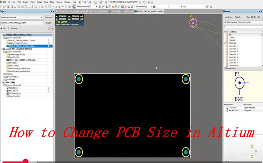
If you are working with Altium Designer, knowing how to change PCB board size in Altium is an important practical skill. Board dimensions may need to be modified when the enclosure changes, component placement is optimized, mounting holes are added, or the original board outline does not meet mechanical requirements.
Altium Designer is widely used for professional PCB Design because it integrates schematic capture, PCB layout, design-rule checking, library management, and manufacturing documentation into a single environment.
Key Considerations for PCB Size in Altium
Before changing the board dimensions, several factors should be reviewed carefully. Changing the PCB outline is not simply a mechanical adjustment; it can affect routing, component clearance, copper areas, impedance control, mounting locations, and manufacturing requirements.
1. Board Shape and Board Outline
The lines that define the physical boundary of a PCB are generally referred to as the board outline or board shape. In Altium Designer, the board shape defines the area recognized as the physical PCB.
All components, tracks, copper pours, and other design elements intended to be fabricated should normally remain within the appropriate board boundaries. Objects extending beyond the board outline may create manufacturing or assembly problems unless they are intentionally designed as part of the product.
A PCB outline can contain straight segments, arcs, rounded corners, circular sections, or customized geometric features. Designers may need to modify the outline when the product enclosure changes or when mechanical constraints require a different board shape.
For complex multilayer PCBs, changing the outline also requires consideration of the internal layer structure. Although the board outline applies to the overall PCB, copper features, vias, planes, and routing on individual layers must still satisfy the required clearances and manufacturing rules.
2. Drawing Objects and PCB Geometry
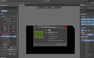
Altium Designer provides a wide range of design objects that can be used to construct and modify PCB geometry. These include tracks, arcs, regions, fills, pads, vias, component footprints, and mechanical-layer objects.
Designers can also create custom shapes and reusable library elements when standard objects are insufficient.
When modifying the board dimensions, these objects should be reviewed carefully. Moving a board edge closer to a component, for example, may violate the required component-to-edge clearance. Similarly, changing the outline may affect copper pours, routing channels, mounting holes, and mechanical features.
Therefore, knowing how to change PCB board size in Altium should always be accompanied by a review of the surrounding PCB layout.
How to Change PCB Board Size in Altium
Changing the PCB size in Altium generally involves editing the board shape rather than simply changing a numerical width or height value. The exact workflow may vary slightly depending on the Altium Designer version and the type of modification required.
1. Prepare and Back Up the PCB Layout
Before changing the board dimensions, save the current PCB file and preferably create a backup or working copy.
This is particularly important when the PCB has already undergone extensive routing and component placement. A significant change to the board outline can require components and traces to be repositioned.
Review the current design before making changes, including:
- Component placement
- Routing
- Copper pours
- Mounting holes
- Keepout regions
- Board-to-edge clearances
- Mechanical features
- Layer stackup
- Manufacturing constraints
Creating a backup allows you to compare the modified design with the original version and restore the previous layout if necessary.
2. Set Units, Origin, and Grid
Before editing the board shape, configure the appropriate measurement units and grid settings.
Altium Designer supports commonly used units such as millimeters and mils. Select the unit system that matches your design requirements and manufacturing documentation.
The coordinate origin is also important when working with precise board dimensions. A suitable origin can make it easier to define the board’s location and measure distances accurately.
The grid should also be selected appropriately. A fine grid can help position board edges, vertices, components, and mechanical features with greater precision.
For example, if the enclosure requires a specific board dimension, using a suitable metric grid can make it easier to maintain consistent dimensions while editing the board outline.
3. Enter the Appropriate PCB Editing Environment
Once the PCB layout has been prepared, open the PCB document in Altium Designer and access the tools used to edit the board shape.
Depending on the version and workflow, board-shape editing functions can be accessed through the Design menu and the board-shape commands.
Before making changes, make sure that you are editing the correct PCB document and that the intended board outline is selected.
For complex designs, designers should also check whether there are multiple board outlines, internal cutouts, or mechanical features that could be affected by the modification.
4. Modify the Existing Board Shape
If only a small adjustment is required, individual segments or vertices of the board outline can be edited.
For example, you may need to:
- Extend one edge
- Shorten an edge
- Move a corner
- Add a vertex
- Modify a rounded corner
- Change an angled section
- Adjust an irregular board profile
Depending on the geometry, you can select and manipulate the relevant board-shape elements.
Altium also provides interactive methods for changing the shape of a board. When working with corners and segments, appropriate editing modes can be used to create straight, angled, or curved transitions.
When modifying a corner, pay attention to the minimum clearance required between the board edge and nearby components, copper features, mounting holes, and other mechanical elements.
5. Redefine the Entire Board Shape
When the entire PCB outline needs to be changed, Altium Designer provides a board-shape redefinition function.
A typical workflow is to use:
Design → Redefine Board Shape
After activating the command, define the new board outline by selecting the required points around the perimeter.
The new outline should form a continuous, closed shape. Once the final point is placed, Altium can create the updated board boundary.
This approach is particularly useful when changing from a rectangular board to a more complex shape or when the PCB must be redesigned to fit a new enclosure.
6. Modify or Add Board-Shape Geometry
In some situations, completely redefining the board is unnecessary. Instead, the existing shape can be modified by adding or adjusting individual elements.
This is useful when the overall board remains similar but one section needs to be extended, shortened, rounded, or reshaped.
For example, a designer may need to create a notch for a connector or add clearance around a mechanical structure.
However, any new geometry should be checked carefully to ensure that the resulting board outline remains closed and manufacturable.
What to Check After Changing PCB Dimensions
Changing the physical dimensions of a PCB can have consequences beyond the board outline itself. After completing the modification, perform a comprehensive design review.
1. Check Component Clearance
Verify the distance between components and the new board edge.
Components located too close to the edge may create problems during PCB assembly, depanelization, soldering, or mechanical installation.
Connectors, switches, large capacitors, heat sinks, and other mechanically sensitive components deserve particular attention.
2. Review Routing
Changing the board dimensions can alter the available routing area.
If the board becomes smaller, traces may need to be rerouted. If the board becomes larger, designers may still need to review whether the routing topology and signal paths remain appropriate.
For high-speed designs, changes to the physical layout can also affect signal integrity, return paths, differential-pair routing, and controlled impedance.
3. Check Copper Pours and Planes
Copper pours and power/ground planes should be reviewed after changing the board outline.
A modified boundary may leave copper areas incorrectly shaped or create unexpected clearances. Repouring the relevant copper regions may therefore be necessary.
For multilayer PCBs, also verify that the plane structure remains consistent with the intended stackup and electrical design.
4. Verify Mounting Holes and Mechanical Features
Mounting holes must remain in the correct locations relative to the new board outline.
Check:
- Hole-to-edge clearance
- Hole diameter
- Mounting-hole coordinates
- Screw and standoff positions
- Connector locations
- Mechanical cutouts
- Enclosure clearance
These mechanical details are especially important when the PCB must fit inside a predefined enclosure.
5. Run Design Rule Checks
After modifying the PCB dimensions, run Altium’s Design Rule Check (DRC).
DRC can help identify issues such as:
- Clearance violations
- Board-edge violations
- Unconnected objects
- Routing problems
- Component placement conflicts
- Manufacturing-rule violations
DRC should not be treated as a replacement for engineering review, but it is an important verification step before releasing the design for PCB Manufacturing.
Best Practices When Changing PCB Size
Several practical considerations can reduce the risk of introducing errors.
- Always create a backup before making major board-outline changes.
- Avoid changing the board dimensions without checking the mechanical requirements.
- Use an appropriate grid for precise positioning.
- Check component-to-edge clearance after every major outline modification.
- Review copper pours and planes after changing the board boundary.
- Verify that the board outline is a closed, continuous shape.
- Check hidden or mechanical-layer objects that may affect the final design.
- Review mounting holes, connectors, cutouts, and enclosure interfaces.
- Run DRC after completing the modification.
- Generate updated manufacturing files only after the revised board dimensions have been fully verified.
For production designs, it is also important to communicate significant dimensional changes to the PCB manufacturer. A modified outline may affect panelization, routing, tooling, fabrication tolerances, and assembly fixtures.
Why PCB Dimensions Matter in PCB Manufacturing
PCB dimensions are not merely a mechanical specification. They influence almost every stage of the manufacturing process.
The board size can affect:
- Panel utilization
- Fabrication yield
- Routing and drilling
- Depanelization
- Assembly equipment compatibility
- Component placement
- Mechanical installation
- Thermal management
- Enclosure integration
A small change in board dimensions may therefore have a larger impact than expected.
For example, reducing the board size can improve product compactness but may reduce routing space and increase component density. Increasing the board size can provide additional routing area but may create mechanical or enclosure constraints.
For this reason, PCB Design and PCB Manufacturing should be considered together rather than treated as completely independent stages.
Conclusion
Knowing how to change PCB board size in Altium is an essential skill for PCB designers. Although changing the board outline may appear to be a simple geometric operation, it can affect component placement, routing, copper pours, mechanical integration, manufacturing tolerances, and PCB assembly.
A reliable workflow should therefore include backing up the original design, configuring the correct units and grid, modifying or redefining the board shape, checking component and mechanical clearances, reviewing routing and copper areas, and finally running DRC.
Before releasing the design for production, the final PCB dimensions should also be verified against the enclosure, manufacturing capabilities, and assembly requirements. Careful control of these parameters can help prevent fabrication errors, unnecessary rework, material waste, and costly production delays.
For businesses that require reliable PCB Manufacturing and PCB assembly support, working with an experienced manufacturing partner such as Kingda can help ensure that the finalized PCB design is translated into a manufacturable and production-ready board.