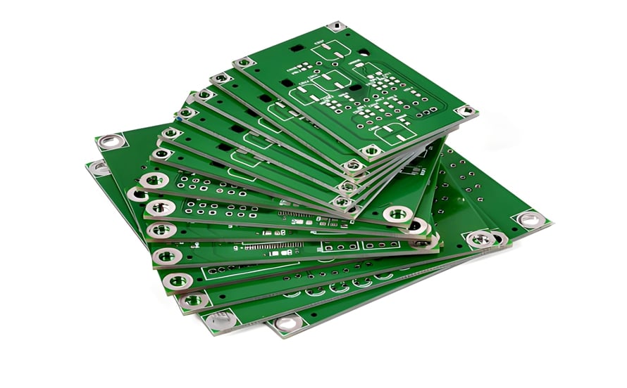
PCB Thickness Guide: Standard Thickness for PCB Design & PCB Manufacturing
The thickness of any physical object refers to the distance from one surface to the opposite surface. Like other mechanical parameters, thickness plays an important role in product design and manufacturing. For printed circuit boards (PCBs), board thickness is equally important because it affects mechanical strength, electrical performance, thermal management, component compatibility, and manufacturability.
So, how thick is a PCB?
In simple terms, PCB thickness is the total distance between the two outer surfaces of the finished board. Depending on the board construction, these outer surfaces may include the solder mask and surface-finish layers over the outer copper. The total thickness is determined by the combined thickness of the laminate, dielectric layers, copper foils, solder mask, and other applicable materials.
Because PCBs are manufactured using stacked layers, their total thickness can be analyzed by looking at the individual materials and layer structures that make up the board. These may include the core, prepreg, copper foil, solder mask, silkscreen, and surface finish.
Modern PCBs are often highly compact, and many standard boards are only a few millimeters thick. However, the appropriate thickness varies considerably depending on the board structure, application, mechanical requirements, and PCB Manufacturing process.
Why Is PCB Thickness Important?
PCB thickness directly affects the mechanical strength and structural stability of a circuit board. A PCB serves as the physical foundation for electronic components and conductive structures, so selecting an appropriate thickness is essential for reliable operation.
A properly specified PCB thickness can help the board:
- Maintain sufficient mechanical rigidity
- Resist bending and vibration
- Fit correctly into connectors and sockets
- Support heavy components
- Meet enclosure and mechanical requirements
- Improve manufacturability
- Provide appropriate thermal performance
- Maintain the required electrical characteristics
For multilayer PCBs, the thickness and dielectric spacing between conductive layers can also influence impedance, capacitance, signal propagation, and overall signal integrity.
PCB Thickness and Thermal Performance
PCB thickness can affect thermal behavior, but thickness alone does not determine how effectively a board dissipates heat.
Copper thickness, copper area, thermal vias, dielectric materials, metal-core structures, component power density, and the surrounding thermal environment can all have a major impact on heat dissipation.
For high-power applications, engineers may use heavier copper, larger copper planes, thermal vias, or specialized PCB materials rather than simply increasing the overall board thickness.
Therefore, PCB thickness should be considered as part of the complete thermal design rather than as an isolated parameter.
Common PCB Thicknesses and Standards
PCB thickness is not governed by a single universal value. Different applications require different board constructions, and manufacturers can produce a wide range of thicknesses.
Nevertheless, several thickness values are commonly encountered in PCB manufacturing.
Typical examples include:
- 0.8 mm
- 1.0 mm
- 1.2 mm
- 1.6 mm
- 2.0 mm
- 2.4 mm
- 3.2 mm
Among these, 1.6 mm is one of the most widely used nominal thicknesses for conventional rigid PCBs.
The actual available thickness depends on the material system, number of layers, copper weights, manufacturing process, and manufacturer’s standard stackups.
PCB Thickness Tolerance
PCB thickness should not be treated as an exact number without tolerance.
Manufacturing processes such as lamination, copper plating, surface finishing, and solder-mask application can introduce dimensional variation. Therefore, the final board thickness should be specified with an appropriate tolerance.
A commonly used tolerance may be around ±10%, although the actual tolerance depends on the PCB manufacturer, board construction, thickness range, and applicable specifications.
For applications requiring tighter mechanical control, engineers may specify tighter tolerances after discussing the requirements with the PCB manufacturer.
What Determines PCB Thickness?
1. Number of PCB Layers
The number of layers is one of the most obvious factors affecting overall PCB thickness.
A multilayer PCB contains multiple copper layers separated by dielectric materials. Additional layers generally require additional core and prepreg structures.
For example, a typical construction may use:
- 2-layer PCB: often around 0.8–1.6 mm
- 4-layer PCB: commonly around 1.2–1.6 mm
- 6-layer PCB: commonly around 1.6–2.0 mm
- 8-layer PCB: often around 1.6–2.4 mm
These are only typical examples rather than fixed standards. A 6-layer PCB can be manufactured at different thicknesses depending on the stackup and application.
For high-density or impedance-controlled designs, the dielectric thickness between signal and reference layers can be more important than simply minimizing total board thickness.
2. Base Material and Copper Weight
Material selection also affects PCB thickness.
A PCB stackup may contain:
- Copper foil
- Core laminate
- Prepreg
- Solder mask
- Surface finish
FR-4 is one of the most widely used rigid PCB materials, but high-speed, high-frequency, flexible, metal-core, and other specialized applications may require different materials.
Copper thickness is another important parameter.
Common copper weights include:
- 0.5 oz
- 1 oz
- 2 oz
- 3 oz
- Heavier copper constructions for high-current applications
Copper weight affects the thickness of individual conductive layers and can also influence current-carrying capability, thermal performance, impedance, and manufacturability.
However, it is important to distinguish copper thickness from total PCB thickness. Increasing copper weight does not necessarily require a proportional increase in total board thickness because the final stackup can be adjusted through the core and prepreg structure.
3. Mechanical Enclosure Requirements
Mechanical constraints often determine how thick a PCB can or must be.
Engineers should consider:
- Enclosure dimensions
- Connector height
- Mounting-hole locations
- Standoff height
- Bracket dimensions
- Component clearance
- Board support points
- Mechanical shock and vibration
Large PCBs are more susceptible to bending and flexing. In such cases, increasing board thickness can improve mechanical rigidity.
However, simply increasing thickness is not always the best solution. Designers can also use mounting points, stiffeners, appropriate board geometry, and optimized mechanical support to control PCB deflection.
4. Thermal and Power Requirements
Thermal and electrical requirements can also influence PCB construction.
High-current applications may require wider traces, larger copper planes, thicker copper, or heavy-copper PCB technology.
For example, power electronics, motor controllers, industrial power supplies, and battery systems may require greater copper cross-sectional area to carry current and reduce resistive losses.
In these applications, the engineering team should evaluate:
- Copper thickness
- Trace width
- Copper plane area
- Current density
- Thermal vias
- Heat dissipation paths
- PCB material
- Component power density
A thicker PCB may improve mechanical stability, but copper thickness and thermal architecture often have a greater influence on current handling and heat dissipation.
5. Manufacturing Tolerances
Every stage of PCB manufacturing has process tolerances.
Processes such as:
- Lamination
- Drilling
- Plating
- Etching
- Routing
- Solder-mask application
- Surface finishing
can affect the final dimensions of the board.
During panelization, the selected board thickness and stackup can also influence how efficiently the PCB can be arranged on a manufacturing panel.
Therefore, designers should establish realistic thickness requirements early in the PCB Design process and confirm the allowable tolerance with the manufacturer.
How to Determine the Right PCB Thickness
Selecting the appropriate PCB thickness requires consideration of both electrical and mechanical requirements.
Consider the Installation Method
First, determine how the PCB will be installed.
Will the board be:
- Mounted inside an enclosure?
- Installed into a card-edge connector?
- Attached to a chassis?
- Fixed with screws and standoffs?
- Installed in a compact consumer device?
- Exposed to vibration or mechanical shock?
The installation method can impose strict thickness requirements.
For example, a PCB that fits into a specific connector must meet the connector’s mechanical specifications. Even a small difference in thickness can affect insertion, retention, or electrical contact.
Consider Component and Connector Requirements
Component height and connector geometry should be evaluated together with PCB thickness.
Important considerations include:
- Connector specifications
- Component clearance
- Mounting-hole dimensions
- Standoff height
- Heat sinks
- Mechanical brackets
- Enclosure clearance
A PCB can meet its electrical requirements but still fail to fit properly into the final product if mechanical requirements are ignored.
Consider Signal Integrity
For high-speed PCB designs, the layer stackup is particularly important.
The distance between a signal layer and its reference plane influences transmission-line impedance. Therefore, designers should not select PCB thickness based only on the overall mechanical thickness.
Instead, the complete stackup should be designed according to:
- Target impedance
- Signal frequency
- Trace width
- Trace geometry
- Dielectric constant
- Dielectric thickness
- Copper thickness
This is particularly important for high-speed digital, RF, and other controlled-impedance applications.
Consider Thermal Requirements
For high-power designs, evaluate the complete thermal system rather than relying solely on board thickness.
Depending on the application, engineers may use:
- Heavy copper
- Large copper planes
- Thermal vias
- Metal-core PCBs
- Heat sinks
- Thermal interface materials
- Improved component placement
These approaches can provide more effective thermal management than simply increasing the overall PCB thickness.
Consider Cost and Manufacturing Capability
A custom PCB thickness may require a customized stackup, which can increase manufacturing complexity and cost.
Whenever possible, designers should consider standard material combinations and manufacturer-supported stackups.
Working with the PCB manufacturer during the design stage can help engineers determine whether the selected thickness is practical for production.
PCB Thickness for Flexible and Rigid-Flex PCBs
Not every PCB is a conventional rigid board.
Flexible PCBs use flexible materials and are generally much thinner than rigid FR-4 PCBs. Their thickness depends on factors such as:
- Number of copper layers
- Copper thickness
- Polyimide thickness
- Coverlay
- Stiffeners
- Adhesive layers
Rigid-flex PCBs combine rigid and flexible sections within a single structure. Consequently, different areas of the same board can have different thicknesses.
When selecting flexible or rigid-flex PCB construction, engineers must also consider bending radius, flexing cycles, stiffener requirements, and mechanical stress.
PCB Thickness and PCB Manufacturing
PCB thickness should be defined during the PCB Design stage rather than left entirely to the manufacturing stage.
A manufacturer needs to understand the required:
- Finished board thickness
- Thickness tolerance
- Layer count
- Copper weight
- Material type
- Surface finish
- Controlled impedance requirements
- Mechanical dimensions
Providing this information early allows the manufacturer to develop an appropriate stackup and identify potential manufacturing issues before production.
For high-volume PCB Manufacturing, using a standard board thickness and a proven material stackup can also simplify production and improve consistency.
Conclusion
PCB thickness is an important parameter in both PCB Design and PCB Manufacturing. There is no single PCB thickness that is suitable for every application. Common rigid PCB thicknesses include 0.8 mm, 1.0 mm, 1.2 mm, 1.6 mm, 2.0 mm, 2.4 mm, and 3.2 mm, but the appropriate value depends on the complete board construction.
When selecting PCB thickness, engineers should consider the number of layers, laminate and dielectric materials, copper weight, mechanical requirements, connector compatibility, signal integrity, thermal requirements, manufacturing tolerances, and cost.
For complex designs, the total board thickness should be considered together with the complete PCB stackup. This is especially important for high-speed, high-power, HDI, RF, flexible, and rigid-flex applications.
By defining the required PCB thickness and tolerance early and confirming the stackup with an experienced manufacturer, engineers can improve manufacturability, mechanical reliability, electrical performance, and overall product quality.
Kingda provides professional PCB Manufacturing and PCB Assembly services for a wide range of PCB structures and applications. Working closely with engineers during the design and manufacturing stages can help ensure that the final PCB meets the required electrical, mechanical, thermal, and production specifications.