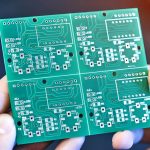
How to Print a PCB: PCB Design & PCB Manufacturing Guide
A Printed Circuit Board (PCB) is the mechanical and electrical platform used to connect electronic components and create functional circuits. Before any electronic product can be manufactured and assembled, its circuit architecture, component placement, and physical layout must be carefully planned.
From compact consumer electronics to advanced industrial, aerospace, and defense systems, PCBs are essential to modern electronic products. The first step is to convert the electrical design into a physical circuit layout that can eventually be manufactured on a PCB.
Technically, “printing a PCB” can refer to different processes. In DIY PCB fabrication, it may mean transferring a circuit pattern onto copper using toner transfer or photoresist. In professional PCB Manufacturing, however, the process is generally based on digital manufacturing data, imaging, photoresist processing, etching, plating, drilling, and other controlled fabrication processes.
This article explains how to print a PCB, including DIY printing methods, professional PCB fabrication, PCB design preparation, circuit pattern transfer, etching, and final board finishing.
What Does Printing a PCB Mean?
PCB printing does not mean printing the complete finished circuit board in the same way a document is printed on paper.
Instead, PCB printing generally refers to transferring a circuit pattern or other graphical information onto a PCB substrate so that the required copper features can be formed or the finished board can be identified.
A typical PCB may contain:
- Copper layers
- Conductive traces
- Component pads
- Vias
- Plated through holes (PTH)
- Surface-mount device (SMD) pads
- Solder mask
- Silkscreen
- Drill holes
- Surface finish
In professional PCB Manufacturing, the circuit pattern is normally generated from PCB design data and transferred to the copper layers through imaging and etching or plating processes.
Understanding this distinction is important when learning how to print a PCB, because DIY printing and industrial PCB fabrication use significantly different equipment and processes.
Types of PCB Manufacturing
DIY PCB Fabrication
DIY PCB fabrication is a practical approach for hobbyists, students, engineers, and small prototype projects.
It typically requires relatively inexpensive tools such as:
- Laser printer
- Glossy transfer paper
- Copper-clad laminate
- Laminator or household iron
- Etching solution
- Drill
- Cleaning materials
DIY manufacturing allows users to quickly create simple prototype PCBs without investing in industrial fabrication equipment.
However, this method has significant limitations. Trace width, spacing, hole accuracy, registration, surface finish, and overall repeatability are generally inferior to professional manufacturing processes.
DIY PCB printing is therefore better suited to simple prototypes, educational projects, and low-density circuits than to production-grade electronics.
Professional PCB Manufacturing
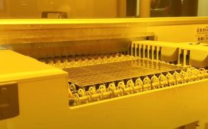
Professional PCB manufacturing uses specialized equipment and tightly controlled processes to produce consistent and repeatable circuit boards.
Depending on the board structure, the manufacturing process may include:
- PCB data preparation
- Material preparation
- Inner-layer imaging
- Etching
- Layer inspection
- Lamination
- Drilling
- Plating
- Outer-layer imaging
- Pattern plating and etching
- Solder mask application
- Surface finishing
- Silkscreen printing
- Electrical testing
- Final inspection
Professional manufacturing is essential when a PCB requires fine-pitch routing, multilayer construction, controlled impedance, high reliability, tight tolerances, or large-scale production.
PCB Printing Methods
Different PCB printing or circuit-pattern-transfer methods can be used depending on the application.
Toner Transfer Method Using a Laser Printer
The toner transfer method is one of the simplest ways to create a PCB prototype at home.
The basic process is:
- Create the PCB layout using PCB design software.
- Mirror the appropriate copper-layer artwork if necessary.
- Print the layout onto glossy transfer paper using a laser printer.
- Clean the copper surface of the PCB.
- Place the printed artwork against the copper surface.
- Apply heat and pressure using an iron or laminator.
- Allow the toner to transfer from the paper to the copper.
- Remove the paper carefully.
- Inspect the transferred pattern.
- Etch away the exposed copper.
The toner acts as an etch-resistant mask. During chemical etching, the copper protected by the toner remains while the exposed copper is removed.
This method is inexpensive and convenient, but it has limited resolution and repeatability. It can be difficult to achieve reliable fine-pitch traces and very small clearances.
Photoresist and UV Exposure
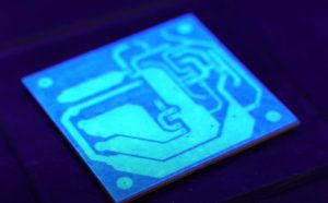
UV exposure is a more precise method for transferring PCB artwork.
In a typical process, the circuit pattern is represented on a transparent film or generated using an appropriate imaging system. A photosensitive resist is applied to the copper surface, and the artwork is aligned with the PCB.
The board is then exposed to ultraviolet light.
Depending on the type of photoresist and process, the exposed or unexposed areas are selectively developed. The resulting resist pattern protects specific areas of copper during subsequent etching or plating.
Compared with toner transfer, photoresist-based processes provide better resolution and are more suitable for complex circuit layouts.
Professional PCB manufacturers use more advanced imaging technologies, including direct imaging systems, to achieve high registration accuracy and fine features.
Professional PCB Printing and Fabrication Process
The complete PCB production process begins with PCB Design and ends with a finished board that is ready for assembly.
It is important to distinguish between the design artwork and the physical manufacturing process. A PCB manufacturer does not simply print a complete circuit onto a copper board. Instead, manufacturing data controls a sequence of imaging, chemical, mechanical, plating, and finishing processes.
PCB Design
Every PCB begins with an electrical and physical design.
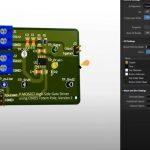
Engineers first create the schematic and then convert it into a PCB layout. Component placement, routing, layer assignment, clearances, via structures, and mechanical dimensions must be carefully considered.
During PCB Design, engineers should verify:
- Component placement
- Trace width
- Trace spacing
- Copper-to-edge clearance
- Pad dimensions
- Via dimensions
- Layer stackup
- Impedance requirements
- Power and ground distribution
- Thermal requirements
- Mechanical dimensions
- Manufacturing tolerances
Design Rule Check (DRC) should be performed before manufacturing data is released.
The final manufacturing package may include Gerber files, drill files, fabrication drawings, stackup information, and other production documentation.
Preparing PCB Manufacturing Data
Once the PCB layout is complete, the design must be converted into manufacturing-ready data.
Gerber files are commonly used to represent individual PCB artwork layers, while drill files provide information about holes and vias.
A typical manufacturing package may include artwork for:
- Top copper
- Bottom copper
- Inner copper layers
- Top solder mask
- Bottom solder mask
- Top silkscreen
- Bottom silkscreen
- Board outline
- Drill data
For complex boards, additional fabrication documentation may specify layer stackup, controlled impedance requirements, surface finish, copper thickness, material type, and dimensional tolerances.
Circuit Pattern Imaging
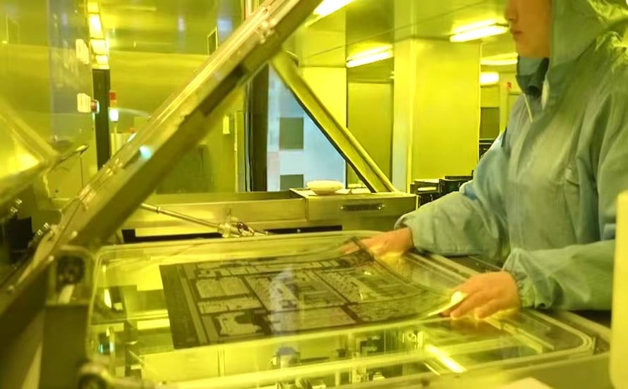
In professional PCB Manufacturing, circuit artwork is transferred to the copper surface using a controlled imaging process.
For many modern PCB factories, photoresist and imaging technologies are used rather than manually “printing” the entire circuit with a conventional printer.
The imaging process creates a defined pattern that determines which copper areas will remain, be plated, or be removed during subsequent processes.
For multilayer PCBs, inner layers must be accurately aligned before lamination. Layer-to-layer registration becomes increasingly important as board density increases.
PCB Etching
After imaging and resist development, the exposed copper can be selectively removed through chemical etching.
The objective is to remove unwanted copper while preserving the required traces, pads, and other conductive features.
The etching process must be carefully controlled because excessive etching can reduce trace width, while insufficient etching can leave unwanted copper between adjacent features.
Important process parameters include:
- Etchant concentration
- Temperature
- Spray pressure
- Conveyor speed
- Copper thickness
- Feature geometry
After etching, the board is cleaned and inspected.
For high-density PCBs, automated optical inspection (AOI) can be used to identify defects such as missing traces, shorts, opens, and pattern deviations.
Drilling and Via Formation
After the required copper structures and layers are formed, holes are drilled according to the manufacturing data.
These holes may include:
- Through holes
- Plated through holes
- Blind vias
- Buried vias
- Mechanical mounting holes
For HDI PCB manufacturing, laser drilling may be used to create microvias.
The drilling process must maintain accurate positioning because even small deviations can affect component mounting, electrical connections, and layer-to-layer registration.
Solder Mask Application
After the copper circuitry has been formed, a solder mask is applied to the PCB.
The solder mask covers most exposed copper while leaving pads and other designated areas available for soldering.
It helps protect the PCB against:
- Oxidation
- Contamination
- Moisture
- Accidental solder bridges
- Mechanical damage
The solder mask also contributes to the visual appearance of the finished PCB.
Surface Finishing
Exposed copper pads normally require a suitable surface finish before component assembly.
Common PCB surface finishes include:
- HASL
- Lead-free HASL
- ENIG
- ENEPIG
- OSP
- Immersion tin
- Immersion silver
The appropriate surface finish depends on factors such as component pitch, solderability, storage requirements, reliability, cost, and application environment.
Silkscreen Printing
The silkscreen is used to print reference designators, polarity marks, component identifiers, logos, warnings, and other information onto the PCB surface.
Unlike copper-layer imaging, silkscreen printing is primarily intended for identification and assembly support.
Typical silkscreen information includes:
- Component reference designators
- Pin-1 indicators
- Polarity markings
- Connector labels
- Product information
- Manufacturer markings
- Warning symbols
Clear silkscreen markings can make PCB assembly, inspection, troubleshooting, and maintenance easier.
Final Cleaning and Inspection
Before PCB assembly, the finished board should be inspected and cleaned according to the manufacturing process requirements.
Inspection may include:
- Visual inspection
- AOI
- Dimensional inspection
- Electrical testing
- Solderability evaluation
- X-ray inspection for selected structures
For production boards, the inspection strategy depends on PCB complexity, application requirements, and quality standards.
DIY PCB Printing vs Professional PCB Manufacturing
The difference between DIY PCB printing and professional manufacturing is significant.
| Feature | DIY PCB Printing | Professional PCB Manufacturing |
|---|---|---|
| Equipment | Basic tools | Specialized production equipment |
| Production Volume | Prototypes and small quantities | Prototype to mass production |
| Trace Resolution | Limited | High precision |
| Layer Count | Usually simple | Multilayer capable |
| Registration | Limited | Controlled and automated |
| Via Technology | Basic | Through, blind, buried, microvia |
| Surface Finish | Limited | Multiple professional finishes |
| Testing | Basic/manual | AOI, electrical testing, X-ray, etc. |
| Repeatability | Relatively low | High |
| Cost per Prototype | Potentially low | Depends on specifications and quantity |
| Production Suitability | Limited | Suitable for commercial production |
The appropriate method depends on the product requirements rather than simply the cost of the initial setup.
Common Mistakes When Printing a PCB
When learning how to print a PCB, several common problems should be avoided.
Incorrect Layer Orientation
When transferring artwork manually, forgetting to mirror the appropriate layer can produce a reversed PCB layout.
Insufficient Trace Width
Extremely narrow traces may be difficult to transfer accurately during DIY fabrication and may also be unsuitable for the required current.
Excessive Trace Spacing
Insufficient clearance between conductive features can result in unintended shorts.
Poor Surface Preparation
Dust, oxidation, oil, and other contaminants can prevent proper toner or photoresist adhesion.
Incorrect Scaling
The printed artwork must maintain its original dimensions. Printer scaling options such as “Fit to Page” can unintentionally change PCB dimensions.
Inadequate Registration
For multilayer boards, poor layer alignment can cause vias and pads to become misregistered.
Ignoring DFM Requirements
A PCB may appear electrically correct but still be difficult or expensive to manufacture.
Designers should therefore review Design for Manufacturing (DFM) requirements before releasing PCB production files.
How to Improve PCB Printing and Manufacturing Results
For reliable PCB production, designers should consider the following practices:
- Use professional PCB design software.
- Set appropriate design rules before routing.
- Use the correct layer stackup.
- Maintain adequate trace width and spacing.
- Verify all component footprints.
- Perform DRC before generating manufacturing files.
- Check Gerber and drill data before release.
- Confirm board dimensions and mounting-hole locations.
- Review DFM requirements with the manufacturer.
- Select appropriate materials and surface finishes.
- Perform electrical and visual inspection after fabrication.
- Keep revision-controlled manufacturing documentation.
These steps reduce manufacturing errors and improve the consistency of the final PCB.
Conclusion
Understanding how to print a PCB is an important part of turning an electronic concept into a physical product. For simple prototypes, toner transfer and UV photoresist methods can provide practical ways to transfer circuit patterns onto copper-clad boards.
For commercial products, however, PCB printing is only one part of a much larger PCB Manufacturing process. Modern production typically combines digital PCB design data, imaging, etching, drilling, plating, solder mask, surface finishing, silkscreen printing, inspection, and electrical testing.
As electronic products become smaller and more sophisticated, PCB layouts require greater routing density, tighter tolerances, better signal integrity, and more advanced manufacturing technologies. Therefore, successful PCB production depends not only on transferring the circuit pattern accurately but also on creating a design that is electrically sound, mechanically reliable, and manufacturable.
For professional PCB projects, Kingda can support the transition from PCB Design data to manufacturing by considering stackup, materials, fabrication tolerances, DFM requirements, and production testing from the early stages of development.