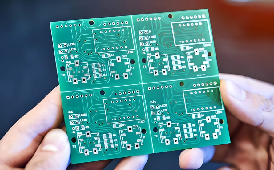
How Many Layers Does a Motherboard PCB Have? PCB Design & PCB Manufacturing Guide
A motherboard is the core and central unit of almost every computing and automation system. The Motherboard PCB is responsible for receiving inputs from external devices or memory, processing data, generating outputs, and supporting data storage for future use. Because modern motherboards must accommodate increasingly complex functions within limited physical dimensions, they commonly use multilayer PCB structures.
This raises an important question during PCB Design: How many PCB layers does a motherboard have?
When discussing PCB layers, engineers typically refer to the conductive copper layers. Other structures, such as solder mask and silkscreen, are considered additional manufacturing layers rather than conductive PCB layers. The copper layers are separated and electrically insulated by dielectric materials within the PCB stackup. Depending on the design, individual layers may be dedicated to signal routing, power distribution, ground reference, or other specialized functions.
This article explains the typical number of layers used in motherboard PCBs, why multilayer structures are necessary, and how engineers approach motherboard PCB stackup design for reliable PCB Manufacturing.
How Many Layers Does a Motherboard PCB Have?
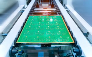
There is no single standard number of layers for every motherboard. The required layer count depends on circuit complexity, component density, operating frequency, power requirements, mechanical constraints, and manufacturing capabilities.
Choosing more layers does not automatically produce a better PCB. The objective is to select the minimum practical layer count that satisfies electrical, mechanical, thermal, and manufacturing requirements.
1. Entry-Level Motherboard PCBs
Simple electronic systems may use a 4-layer PCB as a practical starting point. A typical four-layer stackup may include signal layers on the top and bottom, with internal power and ground layers.
This arrangement provides a relatively simple structure while offering better power distribution and signal integrity than a basic two-layer PCB.
However, as component density, processing performance, and high-speed interfaces increase, four-layer structures can become difficult to route efficiently. As a result, they are less common for sophisticated modern computing platforms.
2. Mid-Range Motherboard PCBs
Many compact and moderately complex systems use 6-layer or 8-layer PCBs. These configurations provide a useful balance between routing capacity, electrical performance, manufacturability, and cost.
In an 8-layer motherboard PCB, for example, several layers can be allocated to high-speed signals, while dedicated or partially dedicated power and ground reference layers improve power distribution and signal integrity.
Additional layers also provide greater flexibility for separating different functional groups. High-speed interfaces, memory buses, power circuits, and lower-speed control signals can be routed more efficiently without consuming excessive space on the external layers.
For many consumer and industrial applications, an 8-layer PCB can provide a practical balance between performance and manufacturing cost.
3. High-End Motherboard PCBs
More complex systems may require 10-layer, 12-layer, 14-layer, 16-layer, or even higher-layer-count PCBs.
These motherboards may support high-speed processors, large memory interfaces, multiple communication standards, high-speed storage, power-management circuits, and numerous peripheral interfaces.
As the number of signals increases, additional layers allow engineers to distribute routing more efficiently across the board. Dedicated ground reference layers can also help control return-current paths and reduce electromagnetic interference.
However, increasing the layer count also makes PCB Design and PCB Manufacturing more demanding. Stackup design, impedance control, via structures, material selection, lamination, registration, and testing all become increasingly important.
4. High-Layer-Count and Specialized Motherboard PCBs
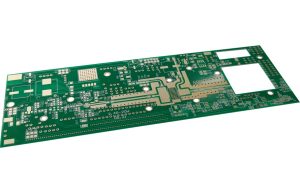
Some advanced computing, telecommunications, aerospace, defense, and other specialized systems may require 20 or more PCB layers.
Such boards are typically designed for extremely high routing density, complex power distribution, multiple high-speed interfaces, or demanding mechanical and reliability requirements.
At this level, every additional layer can significantly affect manufacturing complexity and cost. Engineers therefore need to carefully evaluate whether an additional signal, power, or reference layer is genuinely necessary.
High-layer-count PCB manufacturing also requires tighter process control to manage factors such as layer registration, dielectric thickness, copper distribution, warpage, lamination quality, and via reliability.
Why Do Motherboard PCBs Need Multiple Layers?
The primary reason is that modern motherboards must integrate a large number of electrical functions into a limited physical area.
A multilayer PCB allows engineers to distribute circuits vertically rather than attempting to fit every connection onto the external surfaces. This increases routing capacity while providing controlled reference structures for power and high-speed signals.
Complex Routing
Motherboards contain high densities of SMD components, through-hole components, connectors, and other devices. These components must be interconnected through signal, power, and ground networks.
Trying to route all these connections on only one or two conductive layers would create excessive congestion and complicated crossover requirements.
A multilayer PCB solves this problem by assigning different functions to different layers. Signal routing can be distributed across multiple layers, while power and ground structures occupy internal layers.
This approach can shorten routing paths, reduce congestion, and make high-density layouts more practical.
Power, Ground, and Signal Reference Planes
A motherboard may contain hundreds or thousands of electrical connections, many of which require stable power and ground references.
Using dedicated or partially dedicated power planes and ground planes helps distribute current across the board while providing controlled reference paths for signal layers.
For high-speed signals, a nearby reference plane is especially important. It helps establish a predictable return-current path and supports controlled impedance.
The appropriate layer count therefore depends not only on the number of signal connections but also on how efficiently power and reference planes can be integrated into the stackup.
Impedance Control and Signal Integrity
Impedance control is one of the most important considerations for high-speed motherboard PCB design.
Signals traveling through high-speed interfaces can be affected by trace geometry, dielectric thickness, copper thickness, reference-plane spacing, material properties, and routing environment.
A carefully engineered stackup allows signal layers to be positioned at controlled distances from their reference planes. This makes it easier to achieve the required characteristic impedance.
For example, high-speed differential pairs may require controlled differential impedance, while single-ended interfaces may require a specific characteristic impedance.
An appropriate multilayer structure can therefore help reduce:
- Signal reflection
- Crosstalk
- Electromagnetic interference
- Signal attenuation
- Timing problems
- Return-path discontinuities
Simply adding more layers does not guarantee better signal integrity. The layer arrangement and dielectric structure must be engineered correctly.
Functional Layer Assignment
A motherboard PCB can be divided into functional areas according to circuit requirements.
For example, high-speed memory routing, processor interfaces, power-management circuits, storage interfaces, and lower-speed control signals may require different routing strategies.
Engineers can assign different signal layers to different functional groups while maintaining appropriate reference planes.
This functional organization makes the PCB easier to route and can reduce interference between sensitive circuits.
Vias also provide vertical connections between layers. Depending on the design, engineers may use through vias, blind vias, buried vias, or microvias to improve routing density.
PCB Size and Manufacturability
A compact motherboard must not only function electrically; it must also be manufacturable.
During PCB Design, engineers must consider manufacturing capabilities such as minimum trace width, minimum spacing, via dimensions, aspect ratio, copper thickness, dielectric thickness, layer registration, and lamination requirements.
A theoretically efficient design may still be impractical if its manufacturing requirements exceed the capabilities of the selected PCB manufacturer.
A balanced stackup should therefore provide sufficient routing capacity while maintaining reasonable manufacturing tolerances and production yields.
Motherboard PCB Stackup Design
A multilayer PCB works effectively only when its layers are arranged according to a logical stackup strategy.
The top and bottom layers are generally used for component placement and signal routing. Internal layers can be used for signals, power distribution, and ground references.
Each conductive layer is separated by dielectric material. The dielectric thickness and material properties directly affect impedance, capacitance, signal propagation, and overall electrical performance.
A simplified multilayer motherboard stackup might contain:
| Layer Function | Typical Purpose |
|---|---|
| Top Layer | Components and critical signal routing |
| Inner Signal Layer | High-speed or general signal routing |
| Ground Plane | Signal reference and return-current path |
| Power Plane | Power distribution |
| Inner Signal Layer | Additional routing capacity |
| Ground Plane | Reference and shielding |
| Bottom Layer | Components and signal routing |
The actual stackup depends on the motherboard’s electrical requirements, layer count, materials, copper weights, impedance targets, and manufacturing process.
Via Structures in Multilayer Motherboards
Vias are essential for connecting circuits between different PCB layers.
Through vias extend through the entire board and are relatively straightforward to manufacture. Blind and buried vias can provide greater routing flexibility in high-density designs, while microvias are widely used in HDI structures.
However, advanced via technologies can increase manufacturing complexity and cost. Therefore, via selection should be based on actual routing and density requirements rather than used simply because they are available.
Symmetrical Stackup Design
A symmetrical or balanced stackup can help improve mechanical stability during PCB manufacturing.
Uneven copper distribution or unbalanced dielectric structures can contribute to mechanical stress and warpage during lamination and thermal processing.
For high-layer-count motherboards, engineers therefore need to consider:
- Copper distribution
- Dielectric thickness
- Material symmetry
- Layer registration
- Lamination sequence
- Thermal expansion
- Mechanical stability
It is not simply the number of layers that determines manufacturability; the entire stackup construction matters.
Why PCB Layer Count Affects Manufacturing Cost
Adding PCB layers increases the amount of material, processing, lamination, drilling, registration, inspection, and testing required.
Higher-layer-count boards may also require more advanced technologies, such as:
- Controlled-depth drilling
- Blind and buried vias
- Microvias
- Sequential lamination
- Fine-line routing
- Controlled impedance
- Advanced inspection
- X-ray inspection
- Additional electrical testing
Therefore, increasing the number of PCB layers should not be treated as a simple way to solve routing problems.
During the early stages of PCB Design, engineers should evaluate whether routing congestion can instead be reduced through better component placement, improved layer assignment, optimized via structures, or more efficient power distribution.
The goal is to achieve the required electrical and mechanical performance with an efficient and manufacturable stackup.
Common Factors That Determine Motherboard PCB Layer Count
Several factors influence how many layers a motherboard requires.
Component Density
More components and smaller packages increase routing congestion and may require additional signal layers.
Signal Speed
High-speed interfaces require carefully controlled routing and reference planes. More layers may make it easier to maintain appropriate signal paths.
Power Distribution
High-current processors and other power-hungry circuits may require robust power and ground structures.
Board Size
A smaller board with the same number of connections generally requires greater routing density and may therefore need more layers.
Via Technology
The availability of through vias, blind vias, buried vias, and microvias can significantly affect routing efficiency.
Material Selection
High-speed motherboards may require PCB laminates with controlled dielectric properties and stable electrical characteristics.
Manufacturing Capability
The final layer count must be compatible with the PCB manufacturer’s fabrication capabilities and process tolerances.
How to Choose the Right Number of Motherboard PCB Layers
There is no universal layer count that works for every motherboard.
A practical approach is to:
- Define the electrical and mechanical requirements.
- Estimate the total number of signal connections.
- Identify high-speed interfaces and impedance requirements.
- Determine power and ground distribution requirements.
- Establish the preliminary PCB stackup.
- Assign signal, power, and ground layers.
- Perform placement and routing analysis.
- Check signal integrity and power integrity.
- Review thermal and mechanical requirements.
- Verify manufacturability and production cost.
- Increase the layer count only when necessary.
- Validate the final design through DRC, SI/PI analysis, and appropriate testing.
This process helps prevent both under-designed and unnecessarily expensive PCBs.
Conclusion
Modern motherboards can use anything from 4-layer PCBs to 20-layer or higher-layer-count PCBs, depending on their application and complexity. Entry-level systems may use four layers, while mainstream computing and industrial products commonly require 6, 8, 10, or more layers. Advanced computing, telecommunications, aerospace, and other demanding applications may require significantly higher layer counts.
The number of PCB layers is determined by much more than routing space. PCB Design engineers must consider signal integrity, impedance control, power distribution, component density, thermal performance, mechanical constraints, via technology, material selection, and PCB Manufacturing capabilities.
More layers provide additional routing and reference-plane flexibility, but they also increase material costs, manufacturing complexity, and potential production risks. The objective is therefore not to use as many layers as possible, but to develop an optimized stackup that meets the electrical, mechanical, thermal, reliability, and manufacturing requirements of the final product.
For complex motherboard projects, working with an experienced PCB manufacturing partner such as Kingda can help engineers evaluate stackup options, manufacturing constraints, impedance requirements, and production considerations before moving into mass production.