How to Change PCB Colors in Altium: PCB Design & PCB Manufacturing Guide
PCB Design is the foundation of the final printed circuit board and one of the most critical stages in product development. The PCB layout provides the foundation for subsequent PCB Manufacturing, assembly, testing, troubleshooting, and maintenance.
A PCB layout is developed according to the circuit design, electrical requirements, technical standards, manufacturing capabilities, and intended application. Professional PCB designers typically use EDA software such as Altium Designer to create and manage the layout.
A typical PCB layout contains multiple layers, components, pads, traces, vias, copper areas, mechanical features, and other design objects. When all these objects use similar visual settings, it can become difficult to understand the structure of a complex PCB, especially when working with multilayer designs.
Altium Designer provides extensive visualization controls that allow designers to customize layer colors, system colors, component visibility, and network highlighting. Therefore, learning how to change PCB colors in Altium can significantly improve PCB layout readability and make design review more efficient.
This guide explains how to change PCB colors in Altium’s 2D and 3D views, customize individual net colors, manage visibility settings, and establish an effective color scheme for professional PCB Design.
Altium PCB Color Settings
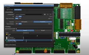
Altium Designer is a comprehensive PCB design platform with numerous visualization and editing functions. Its View Configuration panel provides centralized controls for managing PCB layers, object visibility, system colors, display modes, and other visual settings.
To begin changing PCB colors:
- Open the PCB layout in Altium Designer.
- Open the View Configuration panel.
- Review the available PCB layers and system display options.
- Select the layer or object whose color you want to modify.
- Use the available color controls to assign a new color.
- Apply the changes and review the PCB layout.
The View Configuration panel can also be opened quickly by pressing the L shortcut in the PCB editor.
The exact color options available depend on the current display mode and the type of PCB object being edited.
For example, 2D and 3D views use different visualization controls. Layer colors in the 2D editor are mainly intended to distinguish electrical and design information, while 3D colors can represent physical materials and finished PCB features.
How to Change PCB Colors in 2D View
The 2D PCB editor is the primary environment for PCB layout and routing. It allows designers to view copper layers, solder mask, silkscreen, mechanical layers, component outlines, dimensions, and other design information.
Open the View Configuration Panel
With the PCB editor active, press L to open the View Configuration panel.
You can also access the relevant visualization settings through the PCB editor’s menu system.
The panel provides access to available PCB layers and various system display settings.
Change the Color of a PCB Layer
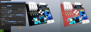
Depending on the Altium version and display configuration, you can access the layer’s color settings through the relevant color control or context menu.
You can then assign a different color to the selected layer.
For example, different colors can be assigned to:
- Top Copper
- Bottom Copper
- Internal signal layers
- Power layers
- Ground-related layers
- Solder mask
- Silkscreen
- Mechanical layers
- Component overlays
Using different colors makes it easier to identify the relationship between layers in a complex multilayer PCB.
Show or Hide PCB Layers
Color customization is only one part of PCB visualization.
You can also control the visibility of individual layers. Hiding unnecessary layers can make routing and design review significantly easier.
For example, when routing the top copper layer, you may temporarily reduce the visibility of other signal layers to focus on the active routing area.
This is particularly useful when troubleshooting dense layouts or reviewing high-speed interfaces.
Adjust Non-Active Layer Appearance
Altium also provides display controls for inactive layers.
Instead of completely hiding other layers, designers can reduce their visual intensity. This allows the active layer to remain prominent while other layers remain visible as references.
This display mode can be useful when reviewing:
- Multilayer routing
- Via transitions
- Differential pairs
- Power distribution
- Component placement
- Layer-to-layer connections
Change the PCB Background
The workspace background can also be customized.
A suitable background can improve contrast between PCB objects and make dense layouts easier to read.
For example, a darker background may provide better visual separation for certain layer colors, while a lighter background may be preferable for documentation or presentation purposes.
Save a Color Configuration
Once a preferred color scheme has been created, the configuration can be saved for future use, depending on the Altium version and available preferences.
A consistent color scheme can be useful when multiple designers work on the same PCB project.
It can also improve design-review efficiency because engineers can quickly recognize specific layers and circuit functions without having to interpret a new color scheme every time.
How to Change PCB Colors in 3D View
Altium’s 3D PCB view provides a more realistic representation of the physical board.
Unlike the 2D editor, which focuses primarily on electrical and layout information, the 3D environment helps designers inspect physical relationships between the PCB, components, connectors, mounting structures, and other mechanical elements.
Switch to 3D PCB View
After opening the PCB layout, switch to the 3D view using Altium’s available 3D display controls or keyboard shortcut.
The 3D view can display physical characteristics such as:
- PCB substrate
- Copper-related structures
- Solder mask
- Silkscreen
- Components
- Connectors
- Mechanical features
Change PCB Material Colors
In the 3D display configuration, physical materials can be represented using different colors.
For example, designers can adjust the visual appearance of the:
- PCB substrate
- Top solder mask
- Bottom solder mask
- Silkscreen
- Components
- Copper-related features
Selecting a color control for a particular material allows the visual appearance to be customized.
It is important to understand that these settings primarily affect visualization. They do not necessarily change the physical material or manufacturing specification of the PCB.
For example, changing the displayed solder mask color in a 3D model does not automatically change the solder mask color specified for PCB Manufacturing.
Adjust Transparency
Transparency can be useful when inspecting hidden structures.
By adjusting transparency, designers can partially reveal components or underlying PCB structures that would otherwise be difficult to see.
This can be helpful when reviewing:
- Internal components
- Component clearances
- Mechanical interference
- PCB mounting areas
- Enclosure interfaces
- Hidden routing relationships
Adjust Lighting and Material Appearance
The 3D environment also provides visualization controls for lighting, reflections, and material appearance.
These settings can make the board easier to inspect from different angles.
For design reviews and presentations, moderate lighting and contrast can make component boundaries and board features more recognizable.
However, visual realism should not be prioritized over engineering clarity. The main purpose of PCB color customization is to improve design interpretation rather than simply make the 3D model look attractive.
How to Change the Color of an Individual PCB Net
Sometimes changing an entire PCB layer is not enough.
A designer may need to highlight a specific network or group of networks, such as:
- VCC
- GND
- CLK
- RESET
- High-speed data lines
- Differential pairs
- Power rails
Altium allows designers to assign visual colors to individual nets so that important connections can be distinguished from surrounding routing.
Select the Required Net
Open the PCB panel and set the relevant navigation or filter mode to Nets, depending on the Altium version and interface configuration.
Locate the desired net in the list.
One or multiple nets can be selected for visualization.
Assign a Net Color
Right-click the selected net and use the available network-color or highlighting controls.
Select the desired color from the available palette.
The selected network can then be displayed using a different color from the default PCB layer appearance.
This is particularly useful when reviewing critical signal paths.
Enable Net Color Override
If the selected network does not appear in the assigned color, check whether the appropriate net-color override or display mode is enabled.
The display configuration determines whether the assigned network color takes priority over the standard layer color.
Refreshing or toggling the relevant display mode may also be necessary if the change does not appear immediately.
Synchronizing Schematic and PCB Network Colors
For complex projects, consistent visualization between the schematic and PCB editors can improve design review.
Network colors can be used to highlight important electrical connections in the schematic and corresponding PCB layout.
When engineering changes are made, project comparison and synchronization functions can help identify differences between schematic and PCB data.
This can be particularly useful for large projects where hundreds or thousands of nets are present.
Consistent color conventions can help engineers quickly identify power, ground, clock, data, and other critical networks across different design environments.
Best Practices for Using PCB Colors in Altium
Color customization should make the design easier to understand rather than introduce additional visual complexity.
1. Use a Consistent Color Scheme
Assign consistent colors to commonly used PCB layers and functions.
For example, designers can establish a standard color convention for top copper, bottom copper, internal signal layers, power layers, and mechanical layers.
2. Use High-Contrast Colors
Colors should provide enough contrast against the workspace background and other PCB objects.
Avoid using several visually similar colors for different layers because this can make layer identification difficult.
3. Highlight Critical Nets
Use network coloring selectively for important signals rather than coloring every net individually.
For example, critical clock signals, power rails, reset signals, and high-speed differential interfaces can be highlighted during design review.
4. Avoid Excessive Color Customization
Using too many colors can make a PCB layout more difficult to understand.
The purpose of color coding is to establish visual hierarchy. A limited and consistent palette is generally easier to interpret than a layout containing dozens of unrelated colors.
5. Use Layer Visibility Effectively
Color changes work best when combined with layer visibility and transparency controls.
When troubleshooting a routing problem, hiding irrelevant layers can be more effective than changing the color of every object.
6. Consider Different Design Views
A color scheme that works well in 2D may not work equally well in 3D.
Therefore, create separate visualization settings appropriate for layout editing, design review, mechanical inspection, and presentation.
7. Keep Manufacturing Information Separate
Remember that Altium’s visualization settings are not necessarily manufacturing specifications.
Changing a layer’s displayed color does not automatically change the physical PCB material, copper thickness, solder mask, surface finish, or other fabrication parameters.
This distinction is especially important when moving from PCB Design to PCB Manufacturing.
Common Problems When Changing PCB Colors in Altium
PCB Color Does Not Change
If the selected object does not change color, check whether another display mode or color override is controlling its appearance.
Also verify that the correct PCB object or layer has been selected.
Colors Are Difficult to Distinguish
If several layers appear similar, choose more contrasting colors and reduce the intensity of inactive layers.
Net Color Is Not Visible
Check whether the net-color override or relevant highlighting mode is enabled.
3D Colors Look Different
3D visualization depends on lighting, reflections, material settings, and viewing angle. Therefore, a color may appear different in 3D compared with the 2D editor.
Color Settings Affect Only the Current Environment
Some visualization settings are associated with the display environment or user preferences rather than the physical PCB manufacturing data.
Therefore, designers should not assume that a display color automatically becomes a manufacturing instruction.
Why PCB Color Management Matters in PCB Design
PCB color management is not merely a cosmetic feature.
A well-organized color scheme can improve:
- PCB layout readability
- Layer identification
- Design review
- Routing efficiency
- Troubleshooting
- Signal tracing
- Design collaboration
- 2D and 3D visualization
- Documentation quality
For complex multilayer boards, visual organization becomes increasingly important because engineers must work with many overlapping routing layers and dense component placement.
Effective color management can therefore become a practical part of the overall PCB Design workflow.
Conclusion
Learning how to change PCB colors in Altium can make PCB layout work significantly easier, especially when working with multilayer and high-density designs.
Altium Designer provides multiple visualization controls through the View Configuration panel, allowing designers to customize layer colors, object visibility, inactive-layer intensity, 3D material appearance, transparency, and individual net colors.
The 2D view is primarily useful for electrical layout and routing, while the 3D view provides a more realistic representation of the physical PCB and its components. Individual net coloring can also be used to highlight critical signals such as power rails, clocks, and high-speed data connections.
However, PCB color settings should be understood as visualization tools rather than manufacturing specifications. Changing a displayed color in Altium does not automatically change the physical PCB material or fabrication requirement.
A well-planned color scheme improves design readability, simplifies design reviews, and helps engineers manage complex layouts more efficiently. When combined with proper DRC, DFM analysis, signal-integrity verification, and manufacturing documentation, effective visualization contributes to a smoother transition from PCB Design to PCB Manufacturing.
For professional PCB projects, Kingda can support engineers from PCB layout review through manufacturing, helping ensure that the final board meets electrical, mechanical, quality, and production requirements.