How to Repair a PCB Pad: PCB Design & PCB Manufacturing Guide
As electronic products become smaller, more compact, and more sophisticated, Printed Circuit Boards (PCBs) must accommodate an increasing number of components within limited space. Every component on a PCB contributes to the overall functionality of the circuit, while the PCB substrate provides the electrical and mechanical foundation that connects these components.
Electronic components are typically soldered to PCB pads, which provide both the electrical connection and the mechanical attachment between the component and the circuit board.
Because pads are exposed to soldering heat, mechanical stress, repeated rework, contamination, and environmental conditions, they can become damaged during PCB assembly, repair, or normal operation. A damaged pad can result in an open circuit, intermittent connection, poor solderability, or complete component failure.
Therefore, understanding how to repair a PCB pad is an important skill for PCB repair and rework technicians.
This guide explains how to identify damaged PCB pads, the common causes of pad failure, and several practical PCB pad repair methods.
How to Identify a Damaged PCB Pad
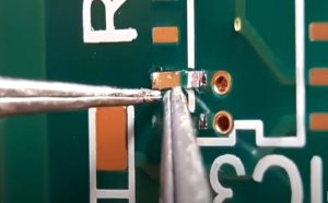
Before attempting any repair, the first step is to determine the type and severity of the pad damage.
A careful inspection can reveal whether the pad is:
- Cracked
- Lifted
- Partially detached
- Burned
- Corroded
- Missing
- Contaminated
- Mechanically damaged
- Electrically disconnected
Visual Inspection
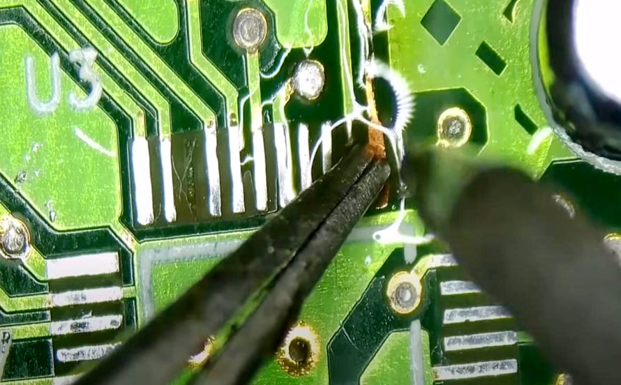
Visual inspection is usually the first step in determining whether a PCB pad is damaged.
For compact or high-density PCBs, a magnifying glass or inspection microscope can make small defects easier to identify.
Look for signs such as:
- Lifted copper
- Cracks around the pad
- Discoloration
- Burn marks
- Corrosion
- Missing solder
- Damaged solder mask
- Separation between the pad and substrate
The surrounding PCB area should also be inspected because pad damage can extend into the connected trace or via.
Electrical and Continuity Testing
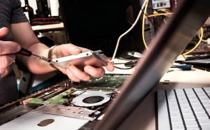
Visual inspection alone cannot always determine whether a pad is electrically functional.
A multimeter can be used to perform continuity and resistance measurements between the pad and its connected trace, via, component pin, or other electrical reference point.
If continuity is missing, the technician should determine whether the failure is caused by:
- A damaged pad
- A broken trace
- A failed via
- A poor solder joint
- An internal PCB connection problem
For complex boards, additional electrical testing may be required.
Mechanical Inspection
A component should never be intentionally stressed to test a PCB pad. Excessive mechanical force can create additional damage.
However, if a component is already loose, careful observation under magnification may reveal movement between the component termination, solder joint, and pad.
This can help identify lifted pads or weak solder joints without unnecessarily damaging the board.
Common Causes of PCB Pad Damage
PCB pads can fail during design, manufacturing, assembly, rework, transportation, or operation.
Understanding the root cause is essential because simply replacing a damaged pad without addressing the underlying problem may result in repeated failure.
PCB Design and Manufacturing Problems
PCB Design determines the dimensions, spacing, geometry, and connection structure of the pads.
Incorrect pad dimensions, insufficient annular ring, inadequate clearance, unsuitable land patterns, or incorrect footprint definitions can contribute to assembly and reliability problems.
Manufacturing issues can also weaken pads. Examples include:
- Poor copper adhesion
- Insufficient copper thickness
- Excessive thermal stress
- Poor plating quality
- Inadequate surface preparation
- Defective solder mask processing
- Lamination problems
When a pad repeatedly fails during assembly, engineers should investigate both the PCB design and manufacturing process rather than assuming that the pad itself is the only problem.
Excessive Heat
Soldering and rework expose PCB pads to elevated temperatures.
If an iron tip is too hot or remains on the pad for too long, excessive heat can weaken the bond between the copper pad and the PCB substrate.
Repeated heating can be particularly damaging.
Excessive thermal exposure may result in:
- Lifted pads
- Delamination
- Damaged solder mask
- Burned laminate
- Weakened copper adhesion
- Damaged nearby components
Proper temperature control and appropriate soldering techniques are therefore essential.
Mechanical Stress
PCB pads can also be damaged by mechanical forces.
Examples include:
- Pulling components from the PCB
- Bending component leads
- Excessive force during connector removal
- Dropping the PCB
- Impact during transportation
- Improper handling
- Excessive pressure on components
Small SMD pads are especially vulnerable because their physical dimensions are relatively small and their connection to the substrate can be weakened by excessive force.
Repeated Desoldering and Rework
PCB assembly and repair may require components to be removed and replaced.
However, repeated soldering and desoldering can gradually weaken the pad and surrounding laminate.
Improper rework techniques, insufficient preheating, excessive soldering temperature, or mechanical pulling can increase the risk of pad lifting.
Controlled heating, suitable flux, appropriate rework tools, and careful component removal can significantly reduce this risk.
Environmental Factors
Environmental exposure can contribute to PCB pad degradation.
High humidity, corrosive chemicals, contamination, and poor storage conditions can promote corrosion of exposed copper and other conductive surfaces.
Contaminated cleaning chemicals or residues from manufacturing and assembly processes can also contribute to corrosion if not properly removed.
In severe cases, corrosion can weaken the copper structure and eventually cause the pad or connected trace to fail.
How to Repair a Damaged PCB Pad
Once the damage has been identified, the appropriate repair method can be selected according to the pad type and severity of the failure.
The repair method for a slightly damaged pad is very different from the method required for a completely missing pad.
Method 1: Rework and Resolder a Slightly Damaged Pad
If the pad is still physically attached to the PCB and the damage is limited to oxidation, contamination, minor solder damage, or a small surface defect, careful rework may be sufficient.
A typical procedure is:
- Inspect the pad under magnification.
- Clean the area with an appropriate PCB-safe cleaning agent.
- Apply a suitable flux.
- Remove excessive or contaminated solder if necessary.
- Re-tin the pad using an appropriate soldering technique.
- Allow the solder to wet the pad properly.
- Inspect the solder joint.
- Perform continuity testing after cooling.
The objective is to restore solderability without applying excessive heat or mechanical force.
This method should not be used if the copper pad has already separated significantly from the substrate.
Method 2: Replace a Severely Damaged Pad
When a pad is completely missing or severely damaged, a replacement pad or copper foil may be installed as part of a professional PCB repair.
The damaged area should first be cleaned and stabilized.
A suitable replacement copper piece can then be shaped to match the original pad geometry.
Depending on the repair method, the replacement may be secured using an appropriate PCB repair adhesive or epoxy system designed for the application.
The replacement pad must then be electrically connected to the appropriate trace or conductive structure.
After curing and final preparation, the component can be soldered to the repaired pad.
The replacement must be carefully aligned because pad dimensions, component pitch, clearance, and connection geometry directly affect the reliability of the repair.
Method 3: Trace or Jumper Wire Repair
If the pad and part of the connected copper trace have been removed, a jumper wire may be required to restore electrical continuity.
A fine insulated wire can be routed from the remaining conductive trace or via to the appropriate component terminal.
The general process is:
- Identify the original electrical connection.
- Locate a suitable point on the remaining trace or via.
- Prepare the connection area.
- Attach a suitable jumper wire.
- Secure the wire mechanically.
- Connect the other end to the component terminal or replacement pad.
- Inspect the solder joints.
- Perform continuity and functional testing.
Although jumper-wire repairs can restore electrical functionality, they may not reproduce the original mechanical strength or high-frequency electrical characteristics of the PCB.
For high-speed, high-current, or safety-critical circuits, the repair should be evaluated against the original electrical and mechanical requirements.
Method 4: Repair a PTH Pad
Through-hole component pads are generally larger than many SMD pads, which can make some repairs easier.
If a PTH pad is partially lifted but the hole and surrounding copper remain usable, the connection may sometimes be repaired through controlled rework.
If the pad is completely missing, a suitable replacement pad or PCB repair method may be required.
For PTH repairs, particular attention should be paid to the plated-through-hole barrel because the electrical connection may extend through multiple PCB layers.
A repair that restores only the surface pad may not restore the internal layer connections.
SMD Pad Repair vs PTH Pad Repair
The repair method depends strongly on the type of pad.
| Feature | SMD Pad Repair | PTH Pad Repair |
|---|---|---|
| Pad Size | Usually smaller | Generally larger |
| Main Challenge | Fine-pitch alignment | Hole and barrel connection |
| Common Damage | Lifted or missing pad | Lifted pad or damaged barrel |
| Repair Difficulty | High for fine-pitch parts | Varies by hole structure |
| Jumper Repair | Common for some cases | Possible when appropriate |
| Layer Connection | Usually surface-level | May connect multiple layers |
| Inspection | Magnification/microscope | Visual and electrical testing |
The technician should identify the original PCB construction before selecting a repair method.
Best Practices for PCB Pad Repair
Following proper repair procedures can reduce the risk of additional damage.
Use Controlled Heating
Avoid excessive soldering temperature and prolonged contact between the soldering iron and PCB pad.
Use a suitable temperature-controlled soldering station and select the appropriate tip for the pad size.
Use Appropriate Flux
Flux can improve solder wetting and reduce oxidation during rework.
However, flux should be compatible with the soldering process and should be cleaned according to the manufacturer’s requirements.
Minimize Mechanical Stress
Never pull a component aggressively from the PCB.
For SMD components, use suitable hot-air, preheating, or rework equipment when appropriate.
Inspect Under Magnification
Small pad defects can be difficult to see with the naked eye.
A microscope or suitable magnification system is particularly useful for fine-pitch components and dense PCB Assembly work.
Match the Original Pad Geometry
When replacing a missing pad, the repair should closely reproduce the original pad dimensions, location, and electrical connection.
Incorrect geometry can result in poor solder joints or component alignment problems.
Secure Repaired Structures
A replacement pad or jumper wire should have sufficient mechanical support for its intended application.
Mechanical fixation can be particularly important when the repaired area will experience vibration or repeated handling.
Clean the PCB After Repair
After soldering and repair, remove flux residues and other contaminants using a cleaning process appropriate for the PCB materials and components.
Test the Repaired PCB
A repaired board should not be returned directly to service without appropriate testing.
Depending on the application, testing may include:
- Continuity testing
- Resistance measurements
- Insulation testing
- Power-up testing
- Functional testing
- Visual inspection
- Signal testing
For complex products, the repaired board should be compared against the original electrical specifications whenever possible.
When Should a PCB Pad Be Repaired or Replaced?
Not every damaged PCB pad should automatically be repaired.
A repair is generally more practical when:
- The PCB is otherwise functional.
- Replacement boards are unavailable.
- The damaged area is localized.
- The board has significant value.
- The repair can restore the required electrical and mechanical performance.
Replacement may be more appropriate when:
- Multiple layers are severely damaged.
- The PCB has extensive delamination.
- Critical internal connections are destroyed.
- The repair would compromise reliability.
- The cost of repair approaches the cost of a replacement PCB.
- The application requires certified or highly controlled manufacturing conditions.
For production products, PCB repair procedures should also be evaluated against applicable quality and reliability requirements.
PCB Pad Repair and PCB Manufacturing Quality
Although PCB pad repair is primarily a rework activity, preventing pad failure begins during PCB Manufacturing.
High-quality PCB fabrication should control factors such as:
- Copper thickness
- Copper adhesion
- Plating quality
- Pad geometry
- Surface finish
- Lamination quality
- Solder mask registration
- Material selection
- Dimensional tolerances
Good PCB Design is equally important.
Appropriate component footprints, pad dimensions, thermal relief design, annular rings, clearances, and manufacturing rules can reduce the likelihood of pad-related problems.
For this reason, pad reliability should be considered throughout the complete PCB lifecycle rather than only after a failure occurs.
Conclusion
PCB pads are small but critical structures that provide both electrical and mechanical connections between components and the circuit board. Because they are exposed to soldering heat, mechanical stress, repeated rework, contamination, and environmental conditions, they can become damaged over time.
Learning how to repair a PCB pad allows engineers and technicians to restore localized damage without necessarily replacing the entire board. Depending on the severity of the damage, repair options may include controlled resoldering, replacement-pad installation, trace repair with jumper wires, or PTH pad repair.
However, successful PCB repair requires more than simply restoring electrical continuity. The repaired area should also provide adequate mechanical strength, solderability, reliability, and performance for the intended application.
The best solution is always to prevent pad damage through proper PCB Design, controlled PCB Assembly, appropriate rework procedures, and high-quality PCB Manufacturing. For professional PCB projects, Kingda can help engineers evaluate PCB design, fabrication, assembly, and quality requirements to reduce the risk of pad-related failures before they reach production.