How to Determine PCB Layers: PCB Design & PCB Manufacturing Guide
With the rapid development of electronics and automation technology, Printed Circuit Boards (PCBs) have become fundamental to almost every modern electronic system. From consumer electronics and industrial automation equipment to automotive systems, aerospace products, and communication devices, PCB technology provides the electrical foundation that connects components and enables complex functions.
As electronic products become smaller, faster, and more functional, PCB designs have evolved from simple single-layer boards to highly integrated multilayer structures. Instead of placing all conductive paths on the top and bottom surfaces, engineers can distribute power, ground, and signal routing across multiple copper layers and connect them through vias.
For engineers involved in maintenance, troubleshooting, repair, or reverse engineering, determining the number and arrangement of PCB Layers is an important first step. Understanding the internal structure of a PCB can help identify hidden connections, analyze failures, reproduce a design, and select an appropriate manufacturing process.
This guide explains how to determine PCB layers using documentation, visual inspection, electrical testing, cross-sectional analysis, software tools, and advanced imaging technologies.
What Are PCB Layers?

A PCB layer is an individual functional layer within a circuit board. Depending on the design, a PCB may contain conductive copper layers, dielectric insulation layers, solder mask, silkscreen, and other structural elements.
In a multilayer PCB, the internal copper layers are separated by dielectric materials. These copper layers may serve different purposes, including:
- Signal routing
- Power distribution
- Ground planes
- High-speed reference planes
- Controlled-impedance transmission lines
The individual layers are laminated together under controlled temperature and pressure during the PCB Manufacturing process. Vias and other interconnection structures provide electrical connections between different copper layers.
PCB configurations range from simple single-layer boards to highly complex multilayer designs containing dozens of copper layers. The required layer count depends on routing density, electrical performance, mechanical requirements, power distribution, signal integrity, thermal requirements, and manufacturing constraints.
For example, a simple consumer product may use a single-layer or two-layer PCB, while industrial controllers and communication equipment commonly require multilayer designs. Advanced aerospace, defense, networking, computing, and high-density applications may require significantly higher layer counts.
Why Is It Important to Determine PCB Layers?
Knowing the layer count is useful in several engineering situations.
During PCB Design, engineers need to understand the stackup to determine where signals, power, and ground are routed. During maintenance, identifying internal layers can help locate hidden connections and potential faults.
Layer identification is particularly important for:
- PCB reverse engineering
- PCB repair and rework
- Failure analysis
- PCB troubleshooting
- Design verification
- Manufacturing inspection
- Stackup reconstruction
- Component and via analysis
- PCB documentation
For a professionally manufactured board, the original design files and fabrication documentation should always be the first source of information. Physical inspection should generally be used when documentation is unavailable or when the actual board needs to be verified.
Methods for Determining PCB Layers
Several methods can be used to identify the number and configuration of PCB Layers. The appropriate method depends on the board structure, available documentation, required accuracy, and whether destructive testing is acceptable.
1. Check the Designer or Manufacturer Documentation
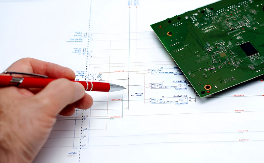
The most reliable and efficient method is to obtain the original design and manufacturing documentation.
A PCB designer or manufacturer may provide information such as:
- Layer count
- PCB stackup
- Copper thickness
- Dielectric materials
- Dielectric thickness
- Board thickness
- Via structure
- Controlled-impedance requirements
- Surface finish
- Material specifications
- Fabrication notes
Native PCB design files can provide significantly more information than manufacturing artwork alone. For example, a native ECAD file may contain layer assignments, routing, component placement, nets, design rules, and stackup information.
Manufacturing files such as Gerber files can also reveal individual copper, solder mask, and silkscreen layers. However, Gerber data is primarily manufacturing artwork and does not necessarily contain the complete logical design or original stackup definition.
Therefore, when available, the original PCB design files, fabrication drawings, stackup documentation, and manufacturer records should be reviewed first.
2. Perform Visual Inspection
Visual inspection is one of the simplest ways to obtain preliminary information about a PCB.
Start by examining both the top and bottom surfaces. Look for:
- Visible copper traces
- Ground areas
- Power planes
- Vias
- Through-hole components
- Blind or buried via structures
- Silkscreen markings
- Test points
- Board-edge features
A magnifier or digital microscope can make small structures easier to identify.
The edge of the PCB can also provide useful clues. In a multilayer board, alternating copper and dielectric regions may sometimes be visible along a properly prepared edge.
However, visual inspection alone cannot reliably determine the complete layer count of a complex multilayer PCB. Internal copper layers are often completely hidden, and surface appearance can be misleading.
Therefore, visual analysis should generally be considered a preliminary method rather than definitive proof.
3. Analyze a PCB Cross-Section
Cross-sectional analysis provides direct information about the internal construction of a PCB.
In a destructive cross-section process, a small portion of the board is removed and mounted for analysis. The exposed surface is then ground and polished before being examined under an optical microscope or, when necessary, a scanning electron microscope (SEM).
A cross-section can reveal:
- Number of copper layers
- Copper thickness
- Dielectric thickness
- Plating thickness
- Via structures
- Lamination interfaces
- Material construction
- Internal defects
This method is especially useful when performing failure analysis, manufacturing verification, or detailed reverse engineering.
Because the process permanently modifies the sample, cross-sectional analysis should be carefully planned when working with a valuable or unique PCB.
4. Use Electrical Tracing and Continuity Testing
Electrical testing can provide valuable information about hidden PCB connections.
A multimeter, continuity tester, or specialized PCB test system can be used to investigate connections between pads, vias, test points, and component terminals.
For example, an engineer may determine whether two points are electrically connected even when the copper trace between them is hidden inside the board.
The process may include:
- Identify accessible pads and vias.
- Test continuity between selected points.
- Record confirmed electrical connections.
- Compare the results with visible routing.
- Identify connections that may pass through internal layers.
- Build a functional map of the board.
This method is particularly useful during PCB Reverse Engineering and repair.
However, continuity testing cannot automatically reveal the exact physical layer of every connection. A confirmed electrical connection only proves that an electrically conductive path exists. Additional evidence may be required to determine its precise location within the stackup.
5. Analyze PCB Design and Manufacturing Files
Digital design and manufacturing files can significantly simplify layer identification.
Depending on the file format, engineers may be able to inspect:
- Copper layers
- Solder mask layers
- Silkscreen layers
- Drill data
- Board outline
- Component placement
- Routing
- Layer assignments
- Stackup information
Modern PCB Design Software can display individual layers independently, making it easier to understand how the board is constructed.
Gerber files are particularly useful for examining the manufacturing artwork of individual layers. Drill files can provide additional information about plated and non-plated holes.
However, engineers should avoid assuming that every file set contains the complete stackup. A collection of Gerber and drill files may describe the manufacturing geometry without fully documenting the dielectric materials, internal layer spacing, or complete design intent.
6. Use Advanced Inspection Methods
When conventional inspection is insufficient, advanced imaging and microscopy can provide additional information.
Common techniques include:
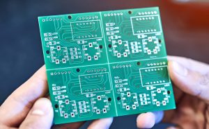
Backlighting
Backlighting can sometimes reveal differences in transparency and internal structures, particularly on thinner or less complex boards. Its effectiveness depends heavily on PCB materials, thickness, copper distribution, and construction.
X-Ray Inspection
X-ray imaging can reveal internal features that cannot be seen from the PCB surface. It is particularly useful for analyzing vias, solder joints, hidden structures, and internal features.
Automated X-ray inspection (AXI) is widely used in electronics manufacturing for inspecting assemblies and detecting certain hidden defects.
CT Scanning
Computed tomography (CT) uses multiple X-ray projections to reconstruct a three-dimensional representation of an object.
For complex PCB structures, CT can provide detailed information about internal geometry without physically cutting the board. It can be particularly useful when analyzing complicated multilayer constructions, hidden vias, or internal mechanical structures.
Optical and Electron Microscopy
Optical microscopy can provide much greater detail than a standard magnifying glass, while SEM can reveal extremely fine structural features at much higher magnification.
These technologies are generally used when high-resolution analysis is required rather than as routine methods for ordinary PCB inspection.
Challenges in Determining PCB Layers
Determining the layer count of a PCB is not always straightforward. Several factors can make the process difficult.
HDI PCB Structures
HDI PCB technology uses fine lines, microvias, blind vias, buried vias, and sequentially laminated structures. These features can make the internal stackup significantly more complicated than that of a conventional multilayer PCB.
Blind and Buried Vias
Blind vias connect an outer layer to one or more internal layers, while buried vias connect internal layers without reaching the external surfaces.
Because these structures are hidden within the board, they can make layer identification considerably more difficult.
Flexible and Rigid-Flex PCBs
A Flexible PCB can have a very different construction from a conventional rigid board. Polyimide layers, copper foils, coverlays, adhesives, and stiffeners may all contribute to the final structure.
A flexible circuit may therefore appear much simpler from the outside than its actual internal construction.
Rigid-flex PCBs can be even more challenging because different sections of the same board may have different layer configurations.
Dense Routing
High-density routing can make it difficult to distinguish individual electrical paths. Multiple vias and closely spaced traces may connect several internal layers in a very small area.
Confusing Components with PCB Layers
Components, shields, stiffeners, thermal structures, and mechanical elements may sometimes be mistaken for PCB layers during a basic visual inspection.
For this reason, layer identification should consider the entire board construction rather than relying on surface appearance alone.
Best Practices for Determining PCB Layers
The following practices can improve accuracy and reduce unnecessary work:
- Always check the original design documentation, fabrication drawing, and stackup information first.
- If documentation is unavailable, request the PCB stackup and manufacturing records from the original manufacturer whenever possible.
- Use visual inspection as an initial screening method rather than the sole source of layer-count information.
- Combine continuity testing with physical inspection during reverse engineering.
- Use PCB design and manufacturing files whenever they are available.
- Record every finding during reverse engineering so that the reconstructed design can be traced and verified.
- Use non-destructive inspection methods before considering destructive cross-section analysis.
- Consult an experienced PCB manufacturer when the stackup or material construction cannot be determined confidently.
- Compare physical findings against electrical behavior and available design data.
- For complex HDI or rigid-flex structures, consider X-ray or CT analysis when conventional methods are insufficient.
PCB Layer Identification and PCB Manufacturing
Accurate layer identification is closely related to PCB Manufacturing.
A multilayer PCB is manufactured according to a defined stackup containing copper foils, cores, prepregs, and other materials. The stackup determines not only the number of layers but also the physical distance between conductive layers.
This information can affect:
- Controlled impedance
- Signal integrity
- Crosstalk
- Power integrity
- Capacitance between planes
- Thermal behavior
- Via design
- Drill requirements
- Manufacturing yield
For high-speed or high-density designs, simply knowing the total number of layers is not enough. Engineers may also need to determine the layer sequence, copper thickness, dielectric thickness, material properties, and via structures.
This is why accurate stackup documentation is an important part of professional PCB Design and manufacturing engineering.
PCB Layer Count vs. Stackup
It is important to distinguish between PCB layer count and PCB stackup.
Layer count describes how many conductive or functional PCB layers are included in the design, while the stackup describes how those layers and dielectric materials are physically arranged.
For example, two six-layer PCBs may both contain six copper layers but use different stackups. One design may prioritize high-speed signal integrity, while another may prioritize power distribution or manufacturing cost.
Therefore, when reverse engineering or reproducing a PCB, identifying the number of layers is only the first step. The actual stackup must also be understood if electrical performance needs to be replicated accurately.
Conclusion
Determining the structure of a PCB is an important skill for PCB Design, troubleshooting, repair, manufacturing verification, and reverse engineering. Simple boards may be analyzed through documentation and visual inspection, while complex multilayer, HDI, flexible, and rigid-flex PCBs may require electrical testing, cross-sectional analysis, X-ray inspection, CT scanning, or microscopy.
The most reliable approach is to combine multiple sources of evidence rather than relying on a single inspection method. Original design documentation and manufacturing records should be prioritized whenever available, followed by non-destructive physical and electrical analysis.
As PCB structures become smaller, denser, and more sophisticated, accurate identification of PCB layers and stackup structures is becoming increasingly important. For engineers and manufacturers such as Kingda, maintaining accurate documentation and understanding the relationship between PCB Design and PCB Manufacturing can improve troubleshooting, repair, reverse engineering, and production reliability.