Custom PCB Manufacturing: PCB Design & PCB Manufacturing Guide
As PCB Technology continues to evolve, printed circuit boards can now be designed and manufactured to meet the increasingly specific requirements of almost any electronic application. The primary function of an electronic circuit is to receive input signals, process them, and generate useful outputs. Every PCB represents a unique electrical system and operates within the limits defined by its circuit architecture, materials, components, and layout.
As modern products become smarter and more multifunctional, users expect more capabilities from a single device. Traditionally, different functions may have required separate PCBs. Integrating multiple independent boards into one product can increase its size, wiring complexity, assembly requirements, and maintenance difficulty.
This is where Custom PCB solutions become valuable.
A custom PCB can integrate multiple functional circuits into a single board or product-level assembly. Different circuit blocks can process multiple inputs, perform specific operations, and generate corresponding outputs. Separate subassemblies can also be interconnected to create a complete customized electronic system.
With an appropriate PCB Design and manufacturing strategy, a custom PCB can provide a more compact, functional, and application-specific solution while reducing unnecessary interconnections between separate boards.
Planning a Custom PCB
Proper planning is one of the most important stages of Custom PCB Manufacturing. A standard PCB requires careful consideration of electrical, mechanical, and manufacturing requirements, while a custom PCB often requires even more analysis before the design begins.
Before starting the schematic, engineers should clearly define the requirements of the final product.
Important questions include:
- What are the maximum PCB dimensions?
- What functions must the PCB perform?
- Is the PCB the final product or a subassembly?
- How will different circuit blocks communicate?
- How will multiple PCB subassemblies be interconnected?
- What are the power requirements?
- Which major components are required?
- What operating temperature and environmental conditions must be supported?
- Are there specific regulatory or industry requirements?
- What production volume is expected?
- What are the expected manufacturing and assembly constraints?
These decisions establish the foundation for the subsequent PCB Design Process.
For example, a compact consumer device may prioritize miniaturization and low power consumption, while an industrial control PCB may require higher reliability, stronger connectors, greater thermal performance, and more robust protection against environmental conditions.
Defining these requirements early can prevent expensive design changes later in the development cycle.
Custom PCB Layout Design
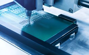
Once the product requirements are finalized, the engineering team can begin the design process.
1. Create the PCB Schematic
The first step is to develop a logical schematic containing all major and supporting components.
The schematic should define:
- Power supplies
- Integrated circuits
- Sensors
- Controllers
- Memory devices
- Communication interfaces
- Connectors
- Protection circuits
- Passive components
- Test points
- Other application-specific circuits
Before moving to layout, engineers should verify the schematic using electrical rules, simulation where appropriate, and design reviews.
This stage is particularly important for a custom PCB because an error in the circuit architecture can affect the entire product.
2. Convert the Schematic Into a PCB Layout
After the schematic has been verified, it is transferred into the physical PCB layout.
The layout must be developed according to the required board dimensions, layer count, stackup, materials, and manufacturing capabilities.
Important layout considerations include:
- Component placement
- Trace width
- Trace spacing
- Routing length
- Via placement
- Power distribution
- Ground planes
- Signal integrity
- Thermal management
- Electromagnetic compatibility
- Clearance requirements
- Connector positioning
- Mounting holes
- Silkscreen information
Both SMD and through-hole components may be used depending on the electrical, mechanical, thermal, and assembly requirements.
For high-speed or high-frequency custom PCBs, additional requirements such as controlled impedance, return-path continuity, differential-pair routing, crosstalk control, and transmission-line effects may need to be considered.
3. Prepare Manufacturing Documentation
Once the layout has been completed and verified, a complete manufacturing package should be prepared.
Typical files and documents include:
- Gerber files
- Drill files
- Pick-and-place files
- Bill of Materials (BOM)
- Assembly drawings
- Fabrication drawings
- Stackup information
- PCB specifications
- Test requirements
- Special manufacturing instructions
For complex custom products, documentation should also clearly define how individual subassemblies are connected and how the final product is assembled.
A complete and consistent manufacturing package helps reduce communication errors between the design team, PCB manufacturer, and assembly provider.
Custom PCB Manufacturing Process
The PCB Manufacturing Process for a custom board generally follows the same fundamental principles as conventional PCB production, but customized requirements may introduce additional materials, processes, inspections, or assembly steps.
1. Select a Suitable PCB Manufacturer
Choosing the right manufacturing partner is one of the most important decisions in custom PCB production.
Not every PCB manufacturer has the same capabilities. Some specialize in high-volume standard boards, while others have stronger capabilities in areas such as:
- Multilayer PCBs
- HDI PCBs
- Rigid-flex PCBs
- High-speed PCBs
- RF and microwave PCBs
- Heavy-copper PCBs
- Metal-core PCBs
- Fine-pitch assembly
- Prototype production
- Low-volume custom manufacturing
When selecting a manufacturer, engineers should evaluate technical capabilities rather than focusing only on price.
Important considerations include:
- Manufacturing capability
- Layer-count capability
- Minimum trace and spacing
- Minimum hole size
- Material availability
- Copper thickness
- Surface-finish options
- PCB assembly capability
- Testing capability
- Quality management systems
- Production capacity
- Engineering support
- Prototype and mass-production support
For complex projects, early communication between the designer and manufacturer can identify potential manufacturing problems before production begins.
2. Select Appropriate Components
Component selection is especially important for custom PCB projects.
Components should be selected according to:
- Electrical specifications
- Package type
- Operating temperature
- Power consumption
- Availability
- Lifecycle status
- Reliability requirements
- Mechanical dimensions
- Manufacturing compatibility
- Cost and expected production volume
Engineers should also consider component obsolescence and supply-chain risks. A component that performs well electrically may still create production problems if it becomes difficult to source.
For custom designs, component selection must also consider interactions between different functional blocks. High-current components, sensitive analog circuits, switching regulators, high-speed interfaces, and RF circuits may require careful physical separation and grounding strategies.
3. Fabricate the PCB
Once the design and manufacturing data have been approved, PCB fabrication begins.
Depending on the PCB type, the manufacturing process may include:
- Material preparation
- Copper-clad laminate preparation
- Inner-layer imaging
- Etching
- Inspection
- Layer alignment
- Lamination
- Drilling
- Through-hole plating
- Outer-layer imaging
- Copper plating
- Etching
- Solder mask application
- Surface finishing
- Silkscreen printing
- Electrical testing
- Final inspection
For multilayer PCBs, individual copper layers are combined with dielectric materials such as prepreg and core materials and laminated under controlled temperature and pressure.
Depending on the design, the PCB may also require blind vias, buried vias, microvias, sequential lamination, or other advanced manufacturing processes.
4. PCB Assembly
After PCB fabrication, components are installed during the PCB Assembly process.
For surface-mount components, solder paste is typically printed onto the appropriate pads. A pick-and-place machine then positions SMD components according to the placement data.
The board passes through a reflow soldering process, where the solder paste is heated according to a controlled thermal profile and forms electrical and mechanical connections between the components and PCB pads.
Through-hole components may be inserted manually or automatically depending on the design and production volume. Wave soldering or selective soldering may be used for suitable through-hole and mixed-technology assemblies.
A custom PCB may contain a combination of:
- SMT components
- Through-hole components
- Connectors
- Cables
- Mechanical hardware
- Shields
- Heat sinks
- Sensors
- Custom modules
The assembly process should be defined together with the PCB layout because component package selection, pad design, component spacing, thermal requirements, and accessibility can directly affect manufacturability.
5. Testing and Troubleshooting
Testing and verification are essential parts of PCB Manufacturing and assembly.
Visual inspection should be performed to identify obvious problems such as:
- Missing components
- Incorrect component orientation
- Solder bridges
- Insufficient solder
- Excess solder
- Component displacement
- Damaged components
- PCB contamination
- Mechanical defects
Depending on the product requirements, additional inspection and testing methods may include:
Automated Optical Inspection (AOI)
AOI systems use cameras and image-processing algorithms to inspect component placement and soldering conditions.
X-Ray Inspection
X-ray inspection can be useful for assemblies containing hidden solder joints, such as BGA and certain QFN packages.
In-Circuit Testing (ICT)
ICT can test electrical characteristics and individual circuit nodes when the product and test fixture are designed to support it.
Functional Testing
Functional testing verifies whether the completed custom PCB performs its intended functions under defined operating conditions.
Environmental and Reliability Testing
Depending on the application, additional testing may include:
- Temperature testing
- Humidity testing
- Thermal cycling
- Vibration testing
- Mechanical shock testing
- ESD testing
- EMC/EMI testing
- Long-duration reliability testing
The specific tests should be selected according to the product’s application, risk level, applicable standards, and customer requirements.
Custom PCB Design Considerations
A successful custom PCB requires more than simply combining several circuits on one board. Engineers should consider the interaction between electrical, mechanical, thermal, and manufacturing requirements.
Electrical Design
Power distribution, grounding, signal integrity, noise, and protection circuits must be carefully designed.
Mechanical Design
Board dimensions, mounting holes, connector locations, component heights, enclosure clearance, and mechanical stress should be considered from the beginning.
Thermal Management
High-power components may require larger copper areas, thermal vias, heatsinks, metal-core construction, or other thermal-management techniques.
Signal Integrity
High-speed interfaces require controlled impedance, appropriate reference planes, short return paths, differential-pair control, and careful via transitions.
Manufacturability
A design that works electrically may still be difficult or expensive to manufacture. Therefore, Design for Manufacturing (DFM) should be incorporated before the final design release.
Serviceability
If the product is expected to be repaired or upgraded, engineers should consider test points, programming interfaces, replaceable modules, diagnostic access, and component accessibility.
Custom PCB vs. Standard PCB
| Feature | Standard PCB | Custom PCB |
|---|---|---|
| Design | Based on defined requirements | Highly application-specific |
| Circuit functions | Usually predefined | Can integrate multiple functional blocks |
| Mechanical requirements | Relatively standardized | Often customized |
| Layer structure | Common configurations | May require specialized stackups |
| Components | Standard selection | Application-specific selection |
| Manufacturing | Established process | May require special processes |
| Testing | Standard test methods | Often customized |
| Production volume | Often medium to high | Prototype to mass production |
| Engineering effort | Moderate | Usually higher |
| Optimization | General-purpose | Optimized for a specific product |
How to Improve Custom PCB Manufacturing
Several practices can improve the efficiency and reliability of custom PCB projects:
- Define electrical and mechanical requirements before starting the layout.
- Involve the PCB manufacturer early in the design process.
- Select components with both performance and supply availability in mind.
- Apply DFM and design-for-assembly principles before production.
- Maintain accurate schematics, BOMs, layouts, and manufacturing documentation.
- Use prototype builds to identify design problems before mass production.
- Define inspection and testing requirements in advance.
- Maintain revision control for hardware and firmware.
- Document all engineering changes.
- Verify the final assembly against the original product requirements.
Conclusion
Custom PCB Manufacturing provides engineers with a way to integrate multiple electronic functions into a compact, application-specific solution. Instead of relying on several independent boards, a carefully engineered custom PCB can combine circuit blocks, power systems, communication interfaces, sensors, controllers, and other functions within a coordinated design.
Successful custom PCB production begins long before fabrication. Requirement analysis, schematic development, component selection, PCB Design, layout optimization, DFM review, fabrication, PCB Assembly, inspection, and functional testing all contribute to the final result.
As electronic products continue to become smaller, smarter, and more integrated, customized PCB solutions will remain important across consumer electronics, industrial automation, automotive electronics, telecommunications, medical equipment, power electronics, and other industries.
For companies such as Kingda, combining engineering expertise with controlled PCB Manufacturing processes can help customers turn application-specific electronic requirements into reliable and manufacturable PCB solutions.