How to Repair a Damaged PCB: PCB Design & PCB Manufacturing Guide
Printed circuit boards (PCBs) are widely used in consumer electronics, industrial equipment, automotive systems, communication devices, medical equipment, and many other applications. Modern PCBs have evolved into highly sophisticated assemblies that integrate hundreds or even thousands of components onto compact substrates.
A PCB substrate is commonly made from materials such as FR-4 fiberglass-reinforced epoxy laminate, although other materials are used for specialized applications. The choice of substrate depends on electrical performance, mechanical requirements, thermal characteristics, operating environment, and overall project cost.
Although PCBs are designed for reliable operation, they can be damaged by mechanical stress, excessive heat, electrical overstress, contamination, moisture, corrosion, improper handling, or manufacturing and assembly defects. Damage may result in failed components, broken traces, lifted pads, damaged vias, delamination, or even cracks through the board.
Fortunately, some PCB damage can be repaired if the underlying structure remains suitable for restoration. This guide explains how to repair a damaged PCB using a systematic inspection, repair, and verification process.
Common Causes of PCB Damage
Understanding the cause of damage is essential before starting a repair. Otherwise, simply replacing a damaged component or repairing a trace may not address the underlying problem.
Common causes include:
Mechanical Stress
Dropping equipment, bending the board, excessive vibration, impact, or improper installation can crack the PCB substrate, break traces, or damage solder joints.
Excessive Heat
High operating temperatures, overheated components, incorrect reflow conditions, or localized thermal stress can damage solder joints, pads, laminates, and components.
Electrical Overstress
Voltage spikes, excessive current, short circuits, electrostatic discharge (ESD), and incorrect power connections can damage components and PCB traces.
Moisture and Contamination
Water, humidity, chemicals, dust, flux residues, and other contaminants can cause corrosion, leakage currents, insulation problems, and degradation of solder joints.
Improper Storage
Heavy stacking, inadequate packaging, uncontrolled humidity, or inappropriate storage conditions can cause mechanical deformation or contamination.
Transportation and Installation
PCBs can be damaged during shipping, connector insertion, screw installation, or mechanical assembly if excessive force is applied.
Identifying the original cause is therefore an important part of PCB Troubleshooting and repair.
How to Repair a Damaged PCB: Step-by-Step Process
PCB repair should be approached as a controlled engineering process rather than simply replacing visible damaged components. The following workflow can help technicians determine whether a board is repairable and restore it safely when appropriate.
1. Prepare the PCB Repair Workstation
PCB repair should be performed in a dedicated and controlled workspace.
A suitable repair workstation may include:
- ESD-safe work surface
- ESD wrist strap and grounding system
- Temperature-controlled soldering iron
- Hot-air rework station
- Desoldering equipment
- Flux and solder
- Solder wick
- Magnification equipment
- Digital microscope
- Multimeter
- Oscilloscope when required
- Laboratory power supply with current limiting
- PCB test fixtures
- Replacement components
- Jumper wires
- Copper foil or repair materials
- Appropriate cleaning materials
The workstation should be properly grounded and free from unnecessary contamination.
Electrostatic discharge can damage sensitive ICs even when there is no visible physical damage. Therefore, ESD protection is particularly important when repairing microcontrollers, memory devices, sensors, communication ICs, and other sensitive components.
2. Inspect and Diagnose the Damage
Before removing anything, perform a detailed inspection of the PCB.
Look for:
- Burn marks
- Cracks
- Broken traces
- Lifted pads
- Missing pads
- Damaged vias
- Corrosion
- Delamination
- Discolored solder mask
- Loose components
- Cracked solder joints
- Damaged connectors
- Swollen or burned components
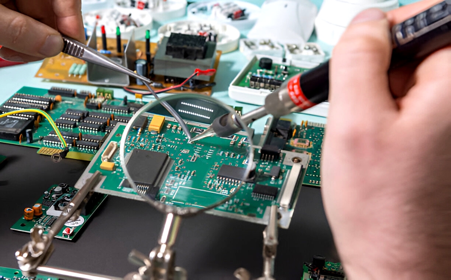
A microscope or digital inspection camera can reveal damage that cannot be identified with the naked eye.
Electrical testing should then be performed where appropriate. Measure resistance, continuity, supply rails, and other relevant electrical parameters.
The key question is:
Is the board actually repairable?
Minor trace damage or a failed discrete component may be relatively straightforward to repair. In contrast, severe multilayer delamination, extensive carbonization, internal layer damage, or damage to safety-critical circuitry may make repair impractical or unreliable.
3. Remove Damaged Components
If damaged components must be replaced, remove them carefully using appropriate rework equipment.
For example:
- Use a temperature-controlled soldering iron for suitable through-hole or accessible SMD components.
- Use hot air for appropriate SMD packages.
- Use specialized equipment for BGA or other complex packages.
- Apply suitable flux when necessary.
- Avoid excessive heating of nearby components and PCB materials.
During desoldering, excessive heat or mechanical force can lift copper pads, damage vias, or delaminate the PCB.
The goal is not simply to remove the failed component but to preserve the surrounding PCB structure so that the replacement can be installed reliably.
4. Clean the PCB
After removing damaged components, clean the affected area when appropriate.
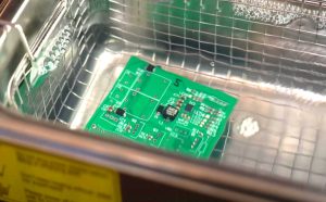
Isopropyl alcohol (IPA) is commonly used for removing certain flux residues and surface contaminants, but the correct cleaning method depends on the PCB materials, flux chemistry, contamination type, and manufacturer requirements.
After cleaning, allow the board to dry completely before applying power.
Cleaning provides several benefits:
- Removes flux residues
- Reduces surface contamination
- Improves visibility during inspection
- Helps identify corrosion or cracks
- Supports reliable soldering and rework
However, cleaning should not be treated as universally mandatory. Some no-clean processes are specifically designed to leave residues under defined conditions. The cleaning process should therefore be compatible with the materials and manufacturing process.
5. Repair Cracked or Physically Damaged PCB Areas
Physical PCB damage requires careful analysis.
For a simple single-layer or double-layer board, a small mechanical crack may sometimes be stabilized and electrically repaired if the damage does not compromise critical structures.
A mechanical repair may involve:
- Removing loose material
- Stabilizing the damaged section
- Using an appropriate PCB repair adhesive or reinforcement method
- Restoring damaged traces separately
- Verifying mechanical strength
However, a crack through a multilayer PCB can be much more serious than it appears from the outside.
A multilayer board may contain internal signal, power, and ground layers that are impossible to inspect visually. A visible crack may therefore interrupt several internal connections or create intermittent faults.
For boards with severe multilayer damage, high-voltage circuits, high-current paths, high-speed interfaces, or safety-critical functions, replacement may be more appropriate than attempting a cosmetic or localized repair.
6. Repair Broken PCB Traces
Broken traces are among the most common PCB repair problems.
The damaged trace should first be inspected and the surrounding solder mask carefully removed to expose clean copper.
Depending on the trace size and electrical requirements, repair methods may include:
- Soldering a short jumper wire
- Using PCB repair wire
- Applying copper foil
- Reconstructing the trace with suitable conductive material
- Reconnecting a damaged via
For a small low-current signal trace, a fine repair wire may be sufficient.
For high-current paths, however, the repair conductor must be appropriately sized to handle the required current and acceptable temperature rise. The repair should also consider voltage drop, mechanical strength, insulation, and clearance.
Simply bridging a large damaged trace with a small piece of wire can create a new reliability problem.
For high-speed signals, the repair becomes more complicated because trace impedance, geometry, return paths, and parasitic effects may affect signal integrity.
7. Repair Damaged PCB Pads
Pads can become lifted, cracked, or completely detached from the PCB due to excessive heat, mechanical stress, repeated rework, or board damage.
A slightly lifted pad may sometimes be stabilized if the copper and underlying laminate remain intact.
A completely missing pad may require a dedicated PCB pad-repair method.
Possible techniques include:
- Copper foil replacement
- Replacement pad material
- Adhesive-supported pad repair
- Trace reconstruction
- Jumper-wire connection
The replacement pad must be positioned accurately and electrically connected to the appropriate trace or via.
Special care is required for:
- Fine-pitch SMD pads
- Thermal pads
- High-current pads
- RF pads
- BGA pads
- Through-hole pads
For a through-hole component, the pad may also be connected to internal layers through a plated hole. Therefore, repairing only the visible surface copper may not restore the original electrical structure.
8. Replace Failed Components
Once the PCB structure, traces, and pads have been repaired, defective components can be replaced.
The replacement component should match the original component’s relevant specifications, including:
- Part number
- Electrical ratings
- Package
- Tolerance
- Temperature rating
- Voltage rating
- Current rating
- Frequency characteristics
- Pin configuration
Component replacement should not be based solely on physical appearance.
For obsolete or unavailable components, an alternative part may sometimes be used, but electrical, mechanical, thermal, and firmware compatibility should be verified before substitution.
9. Test and Validate the Repair
Testing is one of the most important stages of the entire PCB Repair process.
A repaired board should not simply be powered on immediately at full operating voltage.
A controlled verification sequence may include:
- Visual inspection
- Continuity testing
- Resistance checks
- Short-circuit checks
- Power-rail verification
- Current-limited power-up
- Component voltage measurements
- Signal measurements
- Functional testing
- Thermal observation
- Final inspection
A laboratory power supply with current limiting can help reduce the risk of additional damage during the first power-up.
Depending on the application, engineers may also use:
- Multimeters
- Oscilloscopes
- Logic analyzers
- LCR meters
- Electronic loads
- Thermal cameras
- Automated test fixtures
The repaired PCB should be compared with the original design specifications whenever possible.
PCB Repair vs. PCB Replacement
Not every damaged PCB should be repaired.
Repair may be appropriate when:
- Damage is localized.
- Replacement boards are unavailable.
- The PCB has high replacement value.
- The failure is clearly understood.
- The repair can restore the required electrical and mechanical performance.
- The board is not subject to requirements that prohibit or restrict field repair.
Replacement may be more appropriate when:
- The PCB has extensive multilayer damage.
- Internal layers are severely cracked.
- The board has severe delamination or carbonization.
- Safety-critical circuits are affected.
- Repair cannot restore the original electrical characteristics.
- Reliability after repair cannot be adequately verified.
- Repair cost approaches or exceeds replacement cost.
This distinction is particularly important for automotive, medical, aerospace, industrial safety, and other applications where reliability and traceability requirements can be stringent.
PCB Repair and PCB Manufacturing
Although PCB repair and PCB Manufacturing are different processes, they are closely related.
Understanding how a PCB is manufactured helps technicians understand how it can fail and how it should be repaired.
For example, knowledge of:
- PCB stackup
- Copper thickness
- Plated through-holes
- Blind and buried vias
- Solder mask
- Surface finish
- Lamination
- Component assembly
- Thermal management
can make it easier to diagnose physical damage.
The original PCB Design files can also provide important information during repair. Schematics, PCB layouts, Gerber files, drill files, BOMs, and assembly drawings can help engineers identify the original electrical connections and component locations.
This is why proper design documentation is valuable throughout the entire PCB lifecycle.
Best Practices for PCB Repair
The following practices can improve repair quality and reduce the risk of additional damage:
- Identify the root cause before beginning the repair.
- Use ESD-safe equipment when working with sensitive electronics.
- Photograph the board before removing components.
- Record component locations and orientations.
- Keep the original BOM and PCB design data available.
- Use controlled soldering temperatures.
- Avoid unnecessary heating of nearby components.
- Use appropriate wire sizes for trace repairs.
- Verify pad-to-trace and via connections after repair.
- Use current-limited power during initial testing.
- Perform electrical and functional verification before returning the PCB to service.
- Document every repair and component replacement.
- For critical products, follow applicable repair, quality, and traceability procedures.
Conclusion
Learning How to Repair a Damaged PCB requires more than soldering skills. A successful repair depends on accurate diagnosis, knowledge of PCB construction, appropriate rework techniques, careful trace and pad restoration, component replacement, and systematic testing.
Minor problems such as damaged components, broken traces, or lifted pads can often be repaired when the surrounding PCB structure remains intact. However, extensive cracks, delamination, internal-layer damage, severe thermal damage, or safety-critical failures may make replacement a more appropriate solution.
For engineers and technicians, understanding the relationship between PCB Design, PCB Manufacturing, assembly, and repair can make troubleshooting more efficient and improve long-term reliability. At Kingda, a structured approach to PCB engineering, manufacturing, assembly, and quality control can help ensure that repairable boards are restored correctly while boards that cannot reliably be repaired are identified before further resources are invested.