How to Use a PCB in an Electronics Project: PCB Design, PCB Manufacturing & Assembly Guide
Printed circuit boards (PCBs) are the foundation of modern electronics. From small remote-controlled cars and advanced flight-control systems to refrigerators, microwave ovens, and industrial equipment, PCBs are found almost everywhere.
For students, engineers, and electronics enthusiasts, a breadboard is often the first step toward turning an idea into a working circuit. However, anyone who has built a circuit on a breadboard knows how quickly things can become complicated as the number of components and connections increases. Loose jumper wires can make a circuit difficult to troubleshoot, unreliable, and difficult to integrate into a finished product.
Once a circuit has been successfully tested on a breadboard, the next logical step is often to transfer the design to a PCB. A PCB provides permanent electrical connections, a compact structure, and a more reliable platform for integrating electronic components.
This article explains what a PCB is and provides a practical step-by-step guide to PCB Design, PCB Manufacturing, component assembly, and testing, with a particular focus on how to effectively use a PCB in an electronics project.
What Is a PCB?
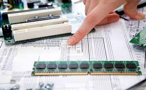
A printed circuit board (PCB) is a flat substrate made from an electrically insulating material, such as FR-4, with conductive copper layers used to create electrical connections between components.
Unlike a breadboard, a PCB does not rely on a network of loose jumper wires. Instead, electrical connections are permanently formed through copper PCB traces, pads, vias, and other conductive structures.
These permanent connections provide several important advantages:
- More reliable electrical connections
- A cleaner and more compact circuit
- Better mechanical stability
- Easier integration into an enclosure or finished product
- Improved repeatability for production
- A more professional appearance
For these reasons, PCB technology is widely used when a prototype needs to move from temporary breadboard testing toward a more reliable and production-ready electronic assembly.
Preparing a PCB for Electronic Components
Once you understand what a PCB is and why it is useful, the next step is learning how to incorporate one into an electronics project.
The process generally includes circuit design, PCB layout, PCB type selection, PCB Manufacturing, component assembly, and electrical testing.
Circuit Design
The first step in creating a PCB is to define the electrical connections between all components. This is normally done by creating a circuit schematic using ECAD software.
Popular PCB design tools include EasyEDA, KiCad, and Altium Designer. These platforms allow engineers and students to create schematics, assign component footprints, check electrical connections, and, in some cases, simulate circuit behavior.
A properly prepared schematic serves as the electrical blueprint for the PCB. It should clearly define components, signal connections, power rails, ground connections, and other important electrical relationships before moving to the PCB layout stage.
PCB Layout Planning
After completing the schematic, the next step is to convert the circuit into a physical PCB layout. Layout planning determines where components are placed and how copper traces are routed across the board.
Although PCB layout is a large subject on its own, several fundamental practices are especially important:
- Place components in a logical arrangement and keep electrically related components close together.
- Place connectors near the edge of the PCB whenever practical to simplify system integration.
- Keep signal traces as short and direct as possible.
- Use wider traces for power and high-current connections when required by the design.
- For complex circuits, consider using a dedicated ground plane instead of routing individual ground traces. Vias can be used to connect the ground plane between PCB layers.
- Provide sufficient space around power components such as MOSFETs, voltage regulators, and power ICs for thermal management.
- Keep sensitive analog or high-speed signal paths away from noisy power or switching circuits when necessary.
A well-planned layout makes the board easier to assemble, reduces the possibility of manufacturing and assembly errors, and improves the overall reliability of the finished circuit.
Choose the Right PCB Type
A PCB can contain one or multiple conductive layers, with each layer serving a specific electrical or mechanical purpose.
The appropriate PCB structure depends on the complexity and requirements of the project. A single-layer PCB may be sufficient for a simple circuit and can provide a cost-effective solution. Double-sided and multilayer PCBs are more suitable for circuits containing microcontrollers, high-speed signals, dense component placement, or complex power and ground networks.
Material selection is also important. Different applications may require different PCB materials and structures, such as:
- Flexible PCB for wearable electronics and applications requiring bending or limited space
- Rigid-flex PCB for compact products requiring both mechanical stability and flexibility
- Aluminum PCB for applications requiring improved thermal management
- High-Tg PCB materials for applications exposed to elevated temperatures
- Specialized high-frequency materials for RF and microwave applications
Selecting the appropriate PCB type during the design stage helps ensure that the finished board can meet the electrical, mechanical, thermal, and environmental requirements of the project.
PCB Manufacturing
After completing the PCB Design and selecting the appropriate materials and layer structure, the design must be prepared for manufacturing.
Most PCB manufacturers require a set of manufacturing files, including Gerber files and drill files, to fabricate the board. These files provide the information needed to manufacture copper layers, solder masks, silkscreens, and drilled holes.
For a professional project, the Gerber files can be reviewed and sent to a qualified PCB manufacturer such as Kingda for fabrication.
For simple educational or hobby projects, some users may also experiment with DIY PCB fabrication methods such as toner transfer and chemical etching. However, professional PCB Manufacturing is generally more suitable when the project requires consistent dimensions, reliable electrical performance, controlled impedance, multilayer construction, or repeatable production quality.
Steps for Using a PCB in an Electronics Project
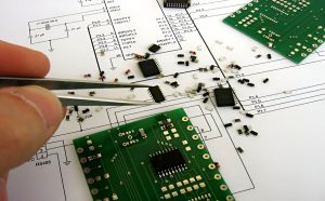
Once the fabricated PCB is available, the next stage is to install the electronic components, solder them to the board, and verify that the circuit works correctly.
The following steps provide a practical overview of how to use a PCB in an electronics project.
1. Gather the Components
The first step is to collect all the components required for the circuit.
ECAD tools such as EasyEDA and Altium Designer can generate a Bill of Materials (BOM) based on the schematic and PCB design. A BOM typically contains information such as component references, part numbers, values, package types, and quantities.
Using a BOM makes component procurement much easier because it provides a complete checklist of the parts required for assembly. For larger projects, the BOM can also be used to organize sourcing and purchasing activities.
Before beginning assembly, verify that the components match the required specifications and package types. This is especially important for polarized components, integrated circuits, connectors, and components with similar appearances but different electrical characteristics.
2. Place the Components on the PCB
After gathering the components, place them onto the corresponding footprints on the PCB.
For through-hole components, it is generally convenient to start with smaller and lower-profile components before installing taller components and connectors. This approach makes the board easier to handle during assembly.
For example, components may be installed in an order such as:
- Resistors and small diodes
- Small capacitors
- Integrated circuits or sockets
- Larger capacitors and other taller components
- Connectors and mechanical components
Component orientation must also be checked carefully. Diodes, LEDs, electrolytic capacitors, ICs, and other polarized components must be installed according to the PCB markings and schematic.
For surface-mount assembly, component placement may be performed manually for prototypes or automatically using pick-and-place equipment for larger production volumes.
3. Solder the Components
Soldering creates both mechanical and electrical connections between the components and the PCB.
For manual assembly, a suitable soldering iron with an appropriate tip and high-quality solder should be used. The soldering temperature and contact time should be controlled to avoid damaging components or PCB pads.
A good solder joint should normally have a smooth and properly formed appearance with sufficient solder coverage. Avoid excessive solder because it can create unintended connections between adjacent pads, particularly on fine-pitch components.
Common soldering problems include:
- Cold solder joints
- Insufficient solder
- Excessive solder
- Solder bridges
- Lifted pads
- Poor component alignment
For larger production volumes, automated processes such as SMT assembly, solder paste printing, pick-and-place, and reflow soldering can provide greater consistency and efficiency.
4. Inspect and Test the PCB
After soldering is complete, carefully inspect the entire PCB before applying power.
First, confirm that every component is installed in the correct location and orientation. Pay particular attention to polarized components and integrated circuits.
Next, inspect the solder joints and PCB traces for visible defects. Make sure that adjacent pads are not accidentally connected by solder bridges.
A multimeter can then be used to perform basic electrical checks, including:
- Checking for short circuits between power and ground
- Checking continuity between relevant points
- Verifying power and ground connections
- Checking component connections where appropriate
For more complex PCBs, additional testing methods such as automated optical inspection (AOI), in-circuit testing (ICT), functional testing, or X-ray inspection may be used depending on the product and manufacturing requirements.
Only apply power after the board has passed the necessary visual and electrical checks. This helps reduce the risk of damaging components or the PCB itself.
Once the PCB has been verified, it can be integrated into the final electronics project.
Why Use a PCB Instead of a Breadboard?
Breadboards are extremely useful during the early prototyping stage because components can be inserted and rearranged without soldering. However, they are not always suitable for a final electronic product.
A PCB provides several advantages:
Reliability: Permanent soldered connections are generally more stable than loose jumper-wire connections.
Compact design: PCB traces can route many electrical connections within a relatively small area.
Repeatability: Once a PCB design has been finalized, multiple boards can be manufactured using the same design files.
Mechanical stability: Components are securely attached to the board, making the assembly easier to install inside an enclosure.
Professional integration: A custom PCB can be designed around the dimensions, connectors, mounting holes, and mechanical requirements of the final product.
For these reasons, moving from a breadboard prototype to a PCB is an important transition in many electronics development projects.
Conclusion
A printed circuit board transforms an electronic circuit from a temporary prototype into a more compact, reliable, and professional assembly. The process involves several important stages, from creating the circuit schematic and planning the PCB Design to selecting the appropriate PCB type, completing PCB Manufacturing, assembling components, and testing the finished board.
For students, engineers, and electronics enthusiasts, learning how to build and use a PCB provides valuable practical experience in electronics design and manufacturing. Each PCB project can also provide opportunities to improve circuit layout, component selection, soldering, testing, thermal management, and design-for-manufacturing skills.
Whether you are developing a simple hobby project or preparing a more advanced electronic product, understanding how to effectively use a PCB can help turn a tested circuit concept into a functional and reliable electronic system.