PCB Manufacturing File Types: Gerber, BOM, Drill, Pick-and-Place & Netlist Files
Although PCB manufacturers differ in capabilities, equipment, and technical expertise, they generally rely on standardized PCB Manufacturing processes and data formats. Standardization helps improve production efficiency, consistency, quality control, and communication between PCB designers and manufacturers.
Modern PCB fabrication and assembly have become highly automated and efficient. This automation also depends heavily on the data transferred from the design stage to manufacturing and assembly. But what file types are actually used for a PCB?
Understanding these files is essential because each file provides specific information required to fabricate, assemble, inspect, or test a circuit board.
This article explains the major PCB Manufacturing file types, their functions, and the common challenges engineers should consider when preparing PCB design data for production.
Why Are File Types Important in PCB Manufacturing?
Why is it important to understand the different file types used in PCB production?
A complete PCB Design workflow must eventually produce manufacturing data that can be correctly interpreted by fabrication and assembly equipment. Even an excellent PCB design becomes difficult to manufacture if the manufacturer cannot accurately interpret the output files.
Different files communicate different aspects of the design, including copper patterns, solder mask openings, silkscreen information, drill locations, component positions, electrical connections, and component specifications.
The main reasons PCB file formats are important include the following.
Prevent Costly Manufacturing and Assembly Errors
Using the correct file format with accurate information helps reduce manufacturing and assembly errors.
For example, fabrication data defines copper layers, pad locations, board outlines, and drilling information. If any of this information is missing or incorrect, the manufacturer may produce a board that does not match the original design.
Such errors can result in:
- Material waste
- PCB rework
- Production delays
- Additional engineering work
- Component assembly problems
- Increased manufacturing costs
Therefore, preparing accurate manufacturing files is an essential part of the PCB Design process.
Improve Communication Between Designers and Manufacturers
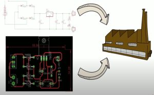
File transfer is the bridge between PCB design and physical production.
PCB designers and manufacturers may use different software platforms and manufacturing systems. Standardized file formats provide a common method for communicating design information between these parties.
A properly prepared manufacturing package allows the manufacturer to understand exactly what the designer intends to produce without relying on assumptions or manually interpreting the original design.
Increase Manufacturing and Assembly Efficiency
Modern PCB manufacturing and assembly equipment can directly process digital manufacturing data.
Accurate files can be imported into CAM systems, CNC drilling machines, solder paste printers, pick-and-place machines, AOI systems, and other automated production equipment.
This reduces manual data entry and helps minimize production errors, improving the overall efficiency of the PCB Manufacturing Process.
Support Quality Control and Inspection
Manufacturing files also provide important references for inspection.
For example, AOI (Automated Optical Inspection) systems compare the manufactured PCB against predefined design data to identify problems such as missing components, incorrect component placement, solder defects, and other assembly issues.
Accurate design output files therefore play an important role in maintaining PCB quality throughout manufacturing and assembly.
What Are the Main PCB Manufacturing File Types?
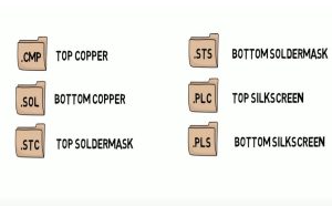
Several file types are commonly included in a PCB manufacturing package. The exact requirements can vary depending on the manufacturer, board complexity, and whether the project involves fabrication, assembly, or both.
The most common files include Gerber Files, NC drill files, BOM files, pick-and-place files, and netlist files.
Gerber Files
Gerber files are among the most important data formats used in PCB fabrication.
Gerber is a standardized CAM data format that represents the graphical information required to manufacture individual PCB layers. Instead of containing the complete editable PCB design, each Gerber file generally represents a specific physical layer or manufacturing feature.
A typical PCB manufacturing package may contain Gerber data for:
- Copper layers
- Solder mask layers
- Silkscreen layers
- Board outline
- Paste layers
- Other fabrication features
Copper Layer Files
Copper Gerber files define the conductive patterns on the PCB, including traces, pads, copper areas, and other features.
For multilayer boards, separate files are generally provided for each copper layer. For example, a four-layer PCB may require individual files for the top copper, inner copper layers, and bottom copper.
These files provide the manufacturer with the graphical information required to create the copper patterns during fabrication.
Solder Mask Files
Solder mask Gerber files define areas where the solder mask should be opened to expose copper pads.
The solder mask helps protect copper traces and reduces the risk of unintended solder bridges during assembly. Accurate solder mask data is therefore important for both PCB protection and soldering quality.
Silkscreen Files
Silkscreen files define markings printed on the PCB surface.
These may include:
- Component reference designators
- Polarity indicators
- Logos
- Assembly instructions
- Identification labels
Correct silkscreen information helps operators identify components and their orientations during PCB assembly and inspection.
NC Drill Files
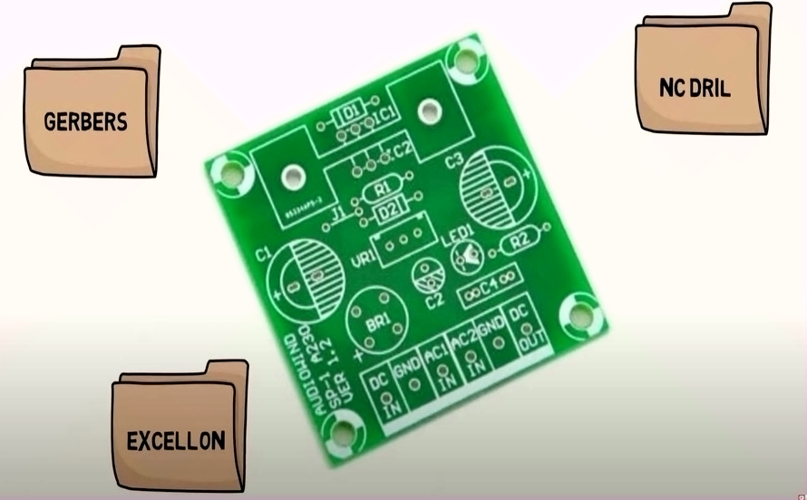
In addition to Gerber files, PCB manufacturers typically require NC drill files to define the holes that must be drilled into the board.
These files specify information such as:
- Hole locations
- Hole sizes
- Hole quantities
- Drill types
- Plated and non-plated hole information, depending on the manufacturing data format
Excellon is a widely used format for PCB drill data, and .drl is a common file extension.
The drill file must correspond correctly with the PCB layout and Gerber data. Any mismatch between the drill data and copper layers can result in incorrect hole locations or manufacturing problems.
What Other File Types Are Used in PCB Manufacturing?
Gerber and drill files are essential for PCB fabrication, but additional files are normally required when the project includes component assembly.
These files provide information about the components, their positions, and their electrical relationships.
Bill of Materials (BOM)
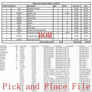
A Bill of Materials (BOM) is a detailed list of the components required to assemble a PCB.
A typical BOM may contain:
- Reference designators
- Manufacturer part numbers
- Component descriptions
- Component values
- Package types
- Supplier information
- Quantities
- Approved alternatives, when applicable
For example, a resistor may be identified by its reference designator, resistance value, tolerance, package size, and manufacturer part number.
The BOM should be kept synchronized with the latest PCB design. If a component is replaced, discontinued, or assigned a new part number, the BOM must be updated accordingly.
An outdated BOM can result in incorrect component procurement or assembly, even when the PCB fabrication files themselves are correct.
Pick-and-Place File
A pick-and-place file, also known as a centroid file or XY file, is primarily used during automated PCB assembly.
It tells the pick-and-place machine where each surface-mount component should be installed.
Typical information includes:
- Reference designator
- X coordinate
- Y coordinate
- Component rotation
- Component side
- Package or footprint information
Accurate pick-and-place data is essential for automated PCB Assembly.
If the PCB layout is modified, the pick-and-place file should also be regenerated to ensure that the component coordinates and orientations remain synchronized with the latest design.
Netlist File
A netlist file describes the electrical connections between components in a PCB design.
It may contain information such as:
- Component names
- Reference designators
- Pin numbers
- Net names
- Electrical connections
The netlist is normally generated from the schematic and can be used as a reference for PCB layout, connectivity verification, and certain manufacturing or testing processes.
Popular PCB design platforms such as Altium Designer, KiCad, and EAGLE can generate or process netlist-related data depending on the design workflow.
Because a netlist represents the intended electrical connectivity, discrepancies between the schematic, netlist, and PCB layout should be identified before manufacturing.
Common Challenges When Transferring PCB Files
Although modern PCB data exchange is highly automated, several problems can still occur during the transfer of manufacturing files.
Identifying these issues before production can help prevent manufacturing delays and unnecessary costs.
Incomplete Gerber Layers
Before sending Gerber files to a PCB manufacturer, designers should verify that all required layers are included.
For example, if a required silkscreen layer is missing from the manufacturing package, the manufacturer may reasonably interpret this as an intentional omission.
A manufacturing checklist should therefore be used to verify that the required copper, solder mask, silkscreen, paste, outline, and other relevant layers are present.
Incorrect Component Positions
Pick-and-place or centroid files may contain incorrect component coordinates if the data was generated from an outdated PCB layout.
This problem can occur when the PCB layout is modified but the assembly files are not regenerated.
To prevent this issue, the latest PCB Design should always be used to generate the final pick-and-place data and other assembly files.
Unclear File Naming
Clear and consistent file naming is important when transferring PCB manufacturing data.
A manufacturing package may contain dozens of files, particularly for a multilayer PCB. Ambiguous names can make it difficult for manufacturers to determine which file corresponds to which layer or manufacturing feature.
A clear naming convention can reduce confusion and improve communication between the PCB designer and manufacturer.
For example, filenames can clearly identify:
- Top copper
- Bottom copper
- Inner copper layers
- Top solder mask
- Bottom solder mask
- Top silkscreen
- Bottom silkscreen
- Board outline
- Drill data
Documentation Problems
A PCB manufacturing package may also contain documentation problems that are unrelated to the basic Gerber geometry.
Examples include:
- Obsolete components
- Missing part numbers
- Incorrect BOM quantities
- Conflicting component specifications
- Missing assembly drawings
- Outdated revision information
These issues can cause assembly problems even when the PCB fabrication files are technically correct.
Therefore, the complete manufacturing package should be reviewed before final release.
How to Prepare PCB Manufacturing Files Correctly
Before sending a PCB project to a manufacturer, designers should perform a final data review.
A practical checklist includes:
- Verify the PCB layout revision.
- Run design-rule checks (DRC).
- Confirm that all required Gerber layers are included.
- Verify the board outline and dimensions.
- Check the NC drill files and hole sizes.
- Review the solder mask and silkscreen layers.
- Confirm that the BOM matches the latest design.
- Regenerate the pick-and-place file after the final layout revision.
- Check component orientations and reference designators.
- Use clear and consistent file names.
- Include fabrication and assembly drawings when necessary.
- Confirm the PCB revision number before releasing the manufacturing package.
This final review helps ensure that the manufacturer receives a complete and internally consistent set of production data.
Conclusion
PCB manufacturing depends not only on a good circuit design but also on accurate and complete manufacturing data. Gerber Files, NC drill files, BOMs, pick-and-place files, and netlists each serve different purposes within the fabrication and assembly workflow.
Understanding these PCB Manufacturing File Types helps engineers communicate more effectively with manufacturers, reduce production errors, improve assembly efficiency, and prevent costly delays.
At Kingda, a reliable manufacturing data package is an essential part of the transition from PCB Design to production. By carefully reviewing every file before manufacturing, designers can create a smoother production workflow and improve the consistency and reliability of the finished PCB.