How to Assemble a PCB: PCB Design, PCB Manufacturing & PCB Assembly Guide
Many breakthrough technologies have transformed the electronics industry. As electronic components and printed circuit boards (PCBs) have become smaller and more compact, bulky electronic equipment has gradually been replaced by lightweight, high-performance products.
The future of electronics depends on continuous innovation in PCB Design, manufacturing processes, materials, component packaging, and production automation. As semiconductor packages and electronic components continue to shrink, PCB assembly processes must also evolve to accommodate finer pitches, higher component densities, and increasingly complex circuit layouts.
Traditional through-hole packages with relatively large leads are increasingly complemented or replaced by smaller surface-mount packages in many applications. As these technologies develop, understanding how to assemble a PCB correctly is essential for achieving reliable electrical connections, consistent quality, and long-term product performance.
This guide explains the major PCB assembly methods, the modern SMT assembly process, important process-control considerations, and common PCB assembly defects.
What Is PCB Assembly?
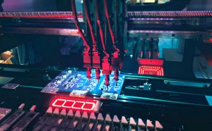
PCB assembly, commonly referred to as PCBA, is the manufacturing process of mounting electronic components onto a bare printed circuit board and creating reliable electrical and mechanical connections between the components and PCB pads.
A typical PCB Assembly process may include solder paste printing, component placement, reflow soldering, inspection, testing, and additional through-hole assembly or rework when required.
PCB assembly takes place after bare-board manufacturing. The bare PCB provides the conductive patterns, pads, vias, and substrate, while assembly transforms that bare board into a functional electronic assembly.
Because modern electronic products use many different component types and package technologies, PCB assembly processes must be adapted to the requirements of each product.
The three major PCB assembly approaches are through-hole assembly, surface-mount assembly, and mixed-technology assembly.
1. Through-Hole PCB Assembly
Through-hole technology (THT) uses components with leads that pass through holes drilled into the PCB.
The leads are inserted through the board and soldered to pads, typically using wave soldering or selective soldering.
Through-hole assembly remains useful for applications that require:
- Strong mechanical connections
- Large components
- High-current connections
- Connectors and switches
- Components exposed to mechanical stress
Although through-hole components generally require more board space than surface-mount components, they can provide excellent mechanical strength.
2. Surface-Mount PCB Assembly
Surface-mount technology (SMT) allows components to be mounted directly onto copper pads on the PCB surface rather than inserting leads through drilled holes.
This approach significantly improves component density and enables much smaller electronic products.
A modern SMT PCB Assembly line commonly includes:
- Solder paste printing
- Pick-and-place
- Reflow soldering
- Automated optical inspection
- X-ray inspection when required
- Electrical testing
SMT is particularly suitable for high-volume production and high-density PCB designs because automated equipment can place thousands of components rapidly and accurately.
3. Mixed-Technology PCB Assembly
Some PCB designs require both surface-mount and through-hole components.
This is known as mixed-technology PCB assembly.
For example, an assembly may use SMT components for compact signal-processing circuits while using through-hole connectors for mechanically demanding interfaces.
Depending on the design, the manufacturing process may combine:
SMT → Reflow Soldering → Through-Hole Insertion → Wave or Selective Soldering → Inspection → Testing
The exact sequence depends on component placement, soldering requirements, thermal limitations, and the board design.
How to Assemble a PCB Using SMT
For modern high-density electronic products, SMT is one of the most widely used PCB assembly technologies.
A typical SMT assembly process consists of several carefully controlled steps.
1. Solder Paste Printing
The first major SMT step is applying solder paste to the PCB pads.
A stencil is positioned over the PCB, and a squeegee moves solder paste across the stencil. The paste passes through precisely defined openings and is deposited onto the corresponding pads.
The quality of solder paste printing has a major influence on final solder-joint reliability.
Important parameters include:
- Stencil thickness
- Aperture dimensions
- Solder paste viscosity
- Squeegee pressure
- Squeegee speed
- PCB alignment
- Stencil cleanliness
For fine-pitch components, even a small variation in solder paste volume or position can lead to solder bridges, insufficient solder, or other assembly defects.
2. Pick-and-Place
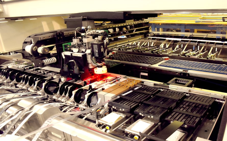
After solder paste printing, automated pick-and-place equipment positions components onto the prepared PCB pads.
The machine retrieves components from feeders and places them according to the PCB assembly data.
Modern placement machines use vision systems to verify component position and orientation.
Important placement parameters include:
- X-Y placement accuracy
- Rotation accuracy
- Component package dimensions
- Feeder configuration
- Nozzle selection
- Component orientation
- Placement speed
Accurate placement is especially important for fine-pitch ICs, small passive components, BGAs, and high-density PCB designs.
3. Reflow Soldering
After component placement, the PCB enters a reflow oven.
During Reflow Soldering, the board passes through controlled temperature zones. The solder paste gradually heats, reaches the required melting temperature, forms solder joints, and then cools under controlled conditions.
A typical reflow profile contains several stages:
- Preheating
- Soaking
- Reflow
- Cooling
The actual temperature profile must be matched to the solder paste, PCB materials, component requirements, and assembly configuration.
Excessive temperature can damage sensitive components or PCB materials, while insufficient heating can result in incomplete soldering.
4. Post-Reflow Inspection
After reflow, the assembled PCB should be inspected to identify potential defects.
Automated Optical Inspection (AOI) can detect visible problems such as:
- Missing components
- Incorrect component orientation
- Component displacement
- Solder bridges
- Insufficient solder
- Excessive solder
- Visible solder defects
X-ray inspection may also be used when solder joints are hidden beneath packages such as BGAs or other bottom-terminated components.
Inspection data can help manufacturers identify process problems before defective boards proceed to subsequent production stages.
Guidelines for Proper PCB Assembly
Understanding how to assemble a PCB is not enough. Manufacturers must also control materials, equipment, process parameters, and inspection procedures.
1. Understand Equipment Capabilities
Every assembly machine has defined mechanical and operational limits.
Before production begins, engineers should understand parameters such as:
- Minimum component size
- Placement accuracy
- Minimum component pitch
- Maximum component height
- PCB dimensions
- Board thickness
- Feeder compatibility
A PCB design should be compatible with the capabilities of the selected assembly equipment.
This is an important aspect of Design for Manufacturing (DFM).
2. Select the Appropriate Solder Paste
Solder paste generally contains metal solder powder, flux, and other formulation components.
The solder alloy and flux chemistry should be selected according to:
- Assembly temperature requirements
- Component sensitivity
- Reliability requirements
- Environmental regulations
- Manufacturing process
- Applicable industry standards
Solder-powder particle size also affects printing performance, especially for fine-pitch applications.
3. Optimize Stencil Design
Stencil design has a direct effect on the amount and location of solder paste deposited on PCB pads.
Important stencil parameters include:
- Stencil thickness
- Aperture size
- Aperture shape
- Pad-to-aperture relationship
- Step-down or step-up areas for mixed components
Fine-pitch components generally require more carefully optimized apertures.
A stencil that is too thick may deposit excessive solder paste, while an overly thin stencil may provide insufficient solder volume for larger components.
4. Optimize the Reflow Profile
The reflow temperature profile is one of the most important parameters in SMT assembly.
The solder paste manufacturer’s technical documentation normally provides recommended heating conditions.
Engineers should verify the actual thermal profile on the PCB rather than relying only on the oven’s programmed temperature.
Thermocouples can be attached to representative locations on the PCB to measure actual board temperatures.
This is particularly important when the board contains:
- Large copper areas
- Heat-sensitive components
- Large thermal masses
- Mixed component sizes
- High-density assemblies
A properly optimized profile helps create consistent solder joints while reducing thermal stress.
Common PCB Assembly Problems
PCB assembly involves many interdependent processes. A problem in solder paste printing, component placement, or reflow can lead to defects later in production.
The following are some common PCB Assembly problems.
1. Solder Bridging
Solder bridging occurs when solder unintentionally connects adjacent pads or terminals.
This can create an electrical short circuit.
Common causes include:
- Excessive solder paste
- Incorrect stencil aperture design
- Poor PCB alignment
- Insufficient spacing
- Excessive paste volume
- Printing problems
Controlling solder paste volume and optimizing stencil design are important ways to reduce this defect.
2. Missing or Misaligned Components
Pick-and-place problems can result in components being missing, incorrectly oriented, or placed outside their intended positions.
Potential causes include:
- Incorrect feeder setup
- Component recognition errors
- Incorrect placement data
- Nozzle problems
- Machine calibration issues
- Component movement during placement
AOI can help identify these defects after assembly.
3. Tombstoning
Tombstoning occurs when one side of a small passive component lifts away from the PCB pad during reflow, leaving the component standing vertically.
This defect is particularly common with small passive components.
Potential contributing factors include:
- Uneven solder paste volume
- Unequal pad heating
- Incorrect pad design
- Poor component placement
- Improper reflow profile
- Differences in thermal mass
Optimizing pad geometry, solder paste deposition, placement accuracy, and the reflow profile can reduce the risk of tombstoning.
4. Solder Balls
Solder balls are small spherical particles of solder that may remain around the PCB after reflow.
They can potentially cause electrical shorts or reliability problems.
Possible causes include:
- Excessive solder paste
- Improper reflow conditions
- Moisture
- Contamination
- Poor stencil printing
- Inappropriate solder paste storage
Maintaining stencil cleanliness and controlling solder paste handling can help minimize solder-ball formation.
5. Insufficient Solder
Insufficient solder occurs when the solder joint does not receive enough solder material to form a reliable connection.
Potential causes include:
- Insufficient paste deposition
- Blocked stencil apertures
- Incorrect stencil thickness
- Poor paste transfer
- Incorrect reflow conditions
SPI (Solder Paste Inspection) can be used before component placement to measure solder paste volume and position, allowing manufacturers to detect problems earlier in the process.
6. Component Damage During Assembly
Components can also be damaged by excessive thermal or mechanical stress.
Sensitive components may require special handling, controlled storage, moisture management, or optimized reflow profiles.
Following component manufacturers’ recommended assembly conditions is essential for maintaining reliability.
How PCB Design Affects PCB Assembly
Successful assembly begins before the PCB reaches the production line.
A well-designed PCB should take manufacturing and assembly requirements into account from the beginning.
Important PCB Design considerations include:
- Component spacing
- Component orientation
- Pad dimensions
- Solder-mask design
- Thermal relief
- Fiducial placement
- Trace-to-pad relationships
- Board edge clearance
- Panelization
- Test-point accessibility
- Component availability
Design for Manufacturing (DFM) and Design for Assembly (DFA) can help identify potential production problems before the PCB enters mass production.
This can reduce manufacturing delays, rework, scrap, and unnecessary production costs.
PCB Assembly Inspection and Testing
Inspection and testing are essential for verifying assembly quality.
Depending on the application and production requirements, a PCB assembly line may use:
- SPI
- AOI
- X-ray inspection
- ICT
- Flying-probe testing
- Functional testing
SPI evaluates solder paste deposition before component placement.
AOI checks visible assembly characteristics after component placement and soldering.
X-ray inspection can inspect hidden solder joints, especially beneath BGA and other concealed packages.
ICT evaluates electrical characteristics at predefined test points.
Functional testing verifies whether the completed PCBA performs its intended electrical functions.
The appropriate testing strategy depends on product complexity, production volume, reliability requirements, and test coverage objectives.
Conclusion
Learning how to assemble a PCB requires an understanding of materials, component packages, soldering technology, equipment capabilities, process control, inspection, and testing.
For modern electronics, SMT assembly provides the high placement density and automation required for compact, high-performance products. Through-hole technology remains valuable where mechanical strength, large components, or high-current connections are required, while mixed-technology assembly combines the advantages of both approaches.
Reliable PCB Assembly begins with a manufacturable PCB Design and continues through controlled solder paste printing, accurate component placement, optimized reflow soldering, inspection, and testing. Careful control of stencil design, solder paste, placement accuracy, and thermal profiles can significantly reduce defects such as solder bridges, tombstoning, solder balls, missing components, and insufficient solder.
For businesses requiring consistent PCB Manufacturing and assembly quality, choosing an experienced manufacturing partner is equally important. Kingda can support PCB production and assembly requirements with professional manufacturing processes designed to help customers achieve reliable, manufacturable, and production-ready electronic assemblies.