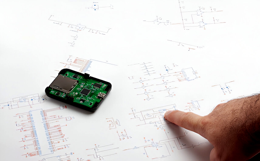
How to Design a PCB: PCB Design, PCB Manufacturing & Step-by-Step Guide
Printed circuit boards (PCBs) are the foundation of countless electronic products and industrial systems. As one of the most important components in an electronic device, a well-designed and properly manufactured PCB can have a significant impact on the product’s electrical performance, reliability, manufacturability, and service life.
For beginners, however, PCB Design can initially seem complicated. A PCB must satisfy electrical, mechanical, thermal, manufacturing, and assembly requirements at the same time. Fortunately, PCB design becomes much easier to understand when it is divided into a structured sequence of steps.
This step-by-step guide explains how to design a PCB, from defining the initial requirements and creating the schematic to developing the layout, verifying the design, preparing manufacturing files, and building a prototype.
What Is PCB Design?
PCB design is the engineering process of converting an electronic circuit concept or schematic into a physical printed circuit board that can be manufactured and assembled.
Whether the project uses a simple single-sided PCB or a complex multilayer PCB, the design process normally includes:
- Defining electrical and mechanical requirements
- Creating the schematic
- Selecting components and footprints
- Creating the board outline
- Designing the PCB layout
- Routing traces
- Defining the layer stackup
- Performing electrical and mechanical checks
- Conducting DRC and DFM reviews
- Preparing manufacturing and assembly documentation
- Building and testing a prototype
The objective is not simply to connect components. A successful PCB Design must also provide adequate signal integrity, power distribution, thermal performance, manufacturability, assembly efficiency, and long-term reliability.
How Is a PCB Designed?
A PCB design workflow should follow a logical sequence. Each stage builds on the previous one, and errors identified late in the process can be significantly more expensive to correct.
The following steps provide a practical introduction for beginners.
1. Define the Purpose and Requirements
Before opening any PCB design software, clearly define what the circuit board needs to accomplish.
The initial requirements may include:
- Electrical functionality
- Supply voltage and current
- Maximum power consumption
- Board dimensions
- Board shape
- Number of PCB layers
- Component types
- Operating temperature
- Mechanical mounting requirements
- Connector locations
- Signal-speed requirements
- EMI/EMC requirements
- Environmental conditions
- Applicable industry standards
- Expected production volume
For example, a low-power consumer device may have very different requirements from an automotive controller, industrial power supply, or high-speed communication board.
A clear requirements document provides a reference for every subsequent design decision and reduces the risk of redesign.
2. Create the Schematic
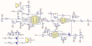
The schematic is the electrical blueprint of the PCB. It defines how components are connected and how the circuit is intended to operate.
Popular EDA platforms such as Altium Designer, KiCad, and OrCAD provide schematic capture tools for developing and checking electronic circuits.
When creating the schematic:
- Place the required components.
- Assign appropriate component values and part numbers.
- Connect components according to the circuit architecture.
- Organize power and ground connections clearly.
- Use appropriate net names and labels.
- Add design notes where necessary.
- Verify component ratings and tolerances.
- Check critical power and signal paths.
- Run Electrical Rules Check (ERC).
Component selection is especially important. The selected component must not only provide the required electrical function but also have a suitable package and footprint for assembly.
The schematic should be electrically complete before the design moves into detailed PCB layout.
3. Design the PCB Layout
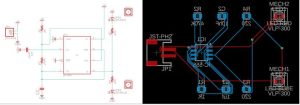
After the schematic has been verified, the next stage is to convert the electrical connections into a physical PCB layout.
This is one of the most important stages of PCB Design because component placement, routing, stackup, grounding, and thermal management can directly affect the performance and manufacturability of the finished board.
Tools such as Altium Designer, KiCad, and OrCAD can be used to create and verify PCB layouts.
Define the Board Configuration
First determine the physical configuration of the PCB.
Important decisions include:
- Board length and width
- Board shape
- Number of copper layers
- PCB material
- Copper thickness
- Finished board thickness
- Via technology
- Surface finish
FR-4 is widely used for general-purpose PCBs, while specialized materials such as PTFE-based laminates may be selected for high-frequency or RF applications.
The required layer count depends on circuit complexity, routing density, signal integrity, power distribution, and EMI requirements.
Place Components Strategically
Component placement should be based on electrical function, signal flow, thermal requirements, mechanical constraints, and assembly considerations.
For example:
- Place connectors according to the mechanical enclosure.
- Keep related functional blocks together.
- Place decoupling capacitors close to their associated IC power pins.
- Keep high-current paths short and wide.
- Separate sensitive analog circuitry from noisy switching circuitry where appropriate.
- Consider heat-generating components during placement.
- Provide adequate clearance for assembly and inspection.
Component placement should be completed before detailed routing begins because poor placement can make routing unnecessarily complicated.
Route PCB Traces
PCB routing establishes the physical conductive paths between components.
Trace width should be selected according to factors such as current, copper thickness, temperature rise, and the manufacturer’s capabilities.
Trace spacing should also account for voltage, manufacturing requirements, electrical safety, and signal integrity.
For high-speed designs, routing requires additional considerations such as:
- Controlled impedance
- Differential-pair routing
- Return-path continuity
- Trace length matching
- Crosstalk
- Via transitions
- Reference-plane continuity
Avoid unnecessary sharp direction changes and excessively long routes. More importantly, routing should preserve appropriate return paths rather than focusing only on making traces as short as possible.
Design the Ground and Power Distribution
A reliable grounding strategy is essential for many PCB applications.
Ground planes can provide low-impedance return paths and help reduce noise when properly implemented. Power distribution should also be designed according to current requirements and voltage-drop limitations.
For multilayer PCBs, dedicated power and ground planes can simplify distribution and improve signal integrity.
However, the exact grounding strategy depends on the circuit architecture. Analog, digital, RF, and high-power circuits may require different approaches.
Define the PCB Stackup
The PCB stackup describes the arrangement of copper and dielectric layers within a multilayer board.
A typical multilayer stackup may include:
- Signal layers
- Ground planes
- Power planes
- Prepreg
- Core materials
- Outer copper layers
The stackup affects:
- Controlled impedance
- Signal integrity
- Power distribution
- Crosstalk
- EMI performance
- Thermal behavior
- Manufacturing cost
For high-speed or RF applications, stackup design should be considered early rather than after routing has already been completed.
The dielectric thickness and material properties between a signal layer and its reference plane directly influence impedance and high-frequency behavior.
4. Verify the PCB Design
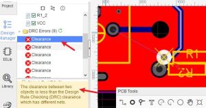
Before sending a design to manufacturing, it must undergo comprehensive verification.
Design verification helps identify errors that may otherwise become expensive manufacturing or assembly problems.
Run Design Rule Checks
Design Rule Check (DRC) software can automatically identify many layout problems, including:
- Insufficient trace spacing
- Trace-width violations
- Clearance violations
- Unconnected nets
- Incorrect hole sizes
- Pad-related problems
- Copper-to-board-edge violations
- Silkscreen clearance problems
However, DRC does not prove that a design is functionally correct. Engineering review is still necessary.
Check Electrical Performance
Depending on the application, electrical verification may include:
- Signal integrity analysis
- Power integrity analysis
- Voltage-drop analysis
- Thermal analysis
- Electromagnetic compatibility considerations
- Controlled-impedance verification
- High-speed simulation
Critical interfaces should be reviewed according to their actual operating conditions rather than relying only on generic design rules.
Check Mechanical Fit
The PCB must fit correctly within the intended enclosure or mechanical system.
Verify:
- Board dimensions
- Mounting holes
- Connector positions
- Component heights
- Keep-out regions
- Edge clearances
- Mechanical interference
A board that works electrically but cannot fit into the final product is not a successful design.
Check Manufacturing Rules
Design for Manufacturing (DFM) should be performed before releasing the design to a fabricator.
Typical DFM considerations include:
- Minimum trace width
- Minimum spacing
- Hole diameter
- Aspect ratio
- Copper-to-edge clearance
- Annular ring
- Solder mask openings
- Silkscreen placement
- Via specifications
- Panelization requirements
The exact limits vary between PCB manufacturers, materials, and production technologies, so designers should obtain the fabricator’s current capabilities before finalizing the design.
Check Assembly Requirements
PCB layout should also support efficient assembly.
Review:
- Component orientation
- Component spacing
- Pick-and-place accessibility
- Solder paste requirements
- Fiducials where required
- Rework accessibility
- Inspection visibility
- Silkscreen readability
The component reference designators should clearly correspond to the physical components and assembly documentation.
5. Prepare PCB Manufacturing Files
Once the design has passed electrical, mechanical, DRC, and DFM reviews, the production documentation can be prepared.
Gerber files are widely used to communicate the artwork for individual PCB fabrication layers, such as:
- Copper layers
- Solder mask
- Silkscreen
- Other required fabrication layers
Drill files provide information about hole locations and sizes.
However, a complete production package normally contains more than Gerber files.
Depending on the project, it may include:
- Gerber or other fabrication artwork
- NC drill files
- Fabrication drawing
- Stackup information
- Board specifications
- Bill of Materials (BOM)
- Pick-and-place/Centroid file
- Assembly drawing
- Assembly instructions
- Testing requirements
The BOM identifies the components required for assembly, while the pick-and-place file provides placement coordinates and orientation information. The assembly drawing communicates component locations and reference designators.
Therefore, Gerber files should not be described as containing the complete component or assembly information.
Communicate With the PCB Manufacturer
Before production, the design package should be reviewed against the manufacturer’s capabilities.
Important topics include:
- Layer count
- Material
- Copper thickness
- Finished thickness
- Minimum trace and spacing
- Minimum drill size
- Surface finish
- Solder mask
- Via technology
- Impedance requirements
- Panelization
- Production quantity
Early communication with the fabricator can identify manufacturing limitations before the design is released.
6. Build and Test a PCB Prototype
A prototype provides an opportunity to validate the design before full-scale production.
Prototype testing may cover several areas.
Electrical Testing
Check whether the PCB performs according to the original electrical requirements.
Depending on the product, this may include:
- Power-up testing
- Voltage and current measurements
- Interface testing
- Functional testing
- Signal integrity testing
- Communication testing
Mechanical Testing
Verify that the PCB fits correctly into the intended product enclosure and interfaces correctly with connectors, brackets, cables, and other mechanical components.
Thermal Testing
Temperature-sensitive components and high-power areas should be evaluated under representative operating conditions.
Thermal testing can help identify:
- Excessive component temperature
- Hot spots
- Inadequate copper area
- Insufficient thermal vias
- Poor heat dissipation
Prototype Evaluation and Revision
Prototype testing frequently reveals issues that were not apparent during schematic and layout review.
Possible improvements may include:
- Component relocation
- Trace-routing changes
- Grounding improvements
- Thermal improvements
- Component substitutions
- Mechanical modifications
- Stackup adjustments
This iterative process helps reduce the risk of expensive problems during mass production.
Common PCB Design Mistakes for Beginners
Beginners can avoid many problems by paying attention to a few common areas.
Poor Component Placement
Random placement often creates unnecessarily long traces, difficult routing, poor thermal performance, and assembly problems.
Insufficient Trace Width
Using traces that are too narrow for the expected current can result in excessive voltage drop or temperature rise.
Ignoring Return Paths
A signal trace should not be considered independently from its return path. Poor return-path design can increase loop area and contribute to signal-integrity and EMI problems.
Inadequate Clearance
Insufficient spacing can cause manufacturing defects, electrical leakage, or unintended shorts.
Ignoring DFM
A PCB can pass electrical checks and still be difficult or expensive to manufacture.
DFM review should therefore be integrated into the design process rather than performed only after the layout is finished.
Incorrect Footprints
An incorrect component footprint can cause assembly failures even when the schematic and electrical connections are correct.
Footprints should be verified against the component manufacturer’s datasheet and package specifications.
Treating DRC as the Final Verification
Automated rule checking is valuable, but it cannot replace engineering judgment.
Functional, thermal, mechanical, and manufacturing reviews are still required.
PCB Design and PCB Manufacturing: Why They Must Work Together
Successful PCB Manufacturing begins with a manufacturable design.
The relationship between design and manufacturing can be summarized as:
Requirements → Schematic → Component Selection → PCB Layout → DRC → DFM → Manufacturing Files → Prototype → Testing → Production
Each stage influences the next.
For example, selecting a smaller package may save board space but make assembly more difficult. Increasing copper thickness may improve current handling but affect etching and manufacturing cost. Adding more PCB layers may simplify routing but increase material and fabrication costs.
Therefore, engineers should consider manufacturability, assembly, testing, and cost while designing the PCB rather than treating manufacturing as a separate final step.
Conclusion
Learning how to design a PCB is a structured engineering process rather than simply drawing traces between components.
The workflow begins by defining electrical, mechanical, environmental, and manufacturing requirements. The designer then creates and verifies the schematic, selects appropriate components and footprints, develops the PCB layout, establishes the stackup, routes signals, and verifies the design through DRC and DFM.
After verification, the required fabrication and assembly files are prepared, the PCB prototype is manufactured, and the design is tested under representative conditions. Any problems discovered during testing can then be addressed before mass production.
A successful PCB Design must therefore balance electrical performance, mechanical requirements, thermal management, signal integrity, manufacturability, assembly, testing, and cost.
By following a systematic design methodology and maintaining close communication between the design team and PCB Manufacturing partner, beginners can gradually develop the skills needed to create reliable, production-ready circuit boards.
Kingda can support PCB fabrication and assembly requirements from prototype development through production, helping customers evaluate manufacturability and production requirements during the transition from PCB design to manufacturing.