How to Connect Components on a PCB: PCB Design, PCB Manufacturing & PCB Assembly Guide
Printed circuit board production and assembly can generally be divided into two major stages: PCB Manufacturing and component assembly. Both stages are essential and require careful planning, accurate execution, and strict quality control. A PCB provides the physical platform for an electronic circuit, while numerous components are mounted on the board and electrically connected through conductive traces.
From a technical perspective, PCB Design determines how electronic components are logically and electrically interconnected through copper traces, pads, and vias. During PCB design, manufacturing, and assembly, engineers must consider component footprints, placement orientation, polarity, pin configuration, and connection points. These factors directly affect electrical performance, assembly efficiency, and product reliability.
Understanding how to correctly connect components on a PCB is therefore an important part of the overall PCB Assembly process. This guide explains the major component mounting technologies and provides a step-by-step overview of how electronic components are connected to a PCB.
What Component Categories and Mounting Technologies Are Used on a PCB?
As PCB technology has evolved, electronic components have become smaller, more integrated, and available in a wider range of package types. The two major component mounting technologies used in PCB assembly are through-hole technology (THT) and surface-mount technology (SMT).
Through-Hole Components
Through-hole components, commonly referred to as PTH or THT components, have leads that pass through holes drilled into the PCB.
During PCB Manufacturing, plated through-holes are created at specific locations according to the PCB layout. The component leads are then inserted through these holes and soldered to conductive pads, usually on the opposite side of the board.
Through-hole technology provides strong mechanical connections and is still widely used for components that require mechanical robustness, high power handling, large connectors, transformers, and certain industrial or power-electronic applications.
Surface-Mount Components
Surface-mount devices (SMDs) are mounted directly onto solder pads on the PCB surface rather than being inserted through drilled holes.
SMD components are generally smaller than comparable through-hole components, allowing engineers to achieve higher component density and more compact product designs. This makes SMT Assembly particularly suitable for modern consumer electronics, telecommunications equipment, automotive electronics, medical devices, and other space-constrained applications.
Instead of inserting leads through the board, an SMD component is accurately positioned on its corresponding pads and permanently attached through a soldering process, typically reflow soldering.
PCB Component Connection Process
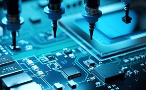
Connecting components to a PCB involves multiple stages, from circuit design and component selection to automated placement, soldering, inspection, and functional testing.
1. Circuit Design and PCB Layout Preparation
Every PCB project begins with a detailed electronic design process.
First, engineers create a schematic based on the electrical requirements of the final product. The schematic defines the electrical relationships between components and identifies the devices required for the circuit.
After the schematic is completed, engineers develop the PCB layout. The layout determines the physical location of components, traces, vias, pads, and other board features.
During this stage, engineers should carefully evaluate:
- Component footprints
- Pin assignments
- Component orientation
- Component polarity
- Electrical ratings
- Clearance requirements
- Thermal requirements
- Signal routing
- Power distribution
- Mechanical constraints
For through-hole components, accurately positioned holes are created in the PCB according to the component footprint. These holes must correspond precisely to the component leads.
For SMD components, appropriately sized copper pads are designed for each component terminal. The pads must maintain the required electrical clearance from adjacent conductive features to prevent unintended connections and potential short circuits.
It is important to note that PCB pads are not necessarily required to remain electrically isolated in every case. Whether two pads are connected depends on the schematic and PCB net assignment. The key requirement is that every connection matches the intended electrical design.
2. Component Placement on the PCB
The component placement method depends on the selected mounting technology and production requirements.
Through-Hole Component Placement
Through-hole components are commonly inserted into the PCB either manually or with specialized insertion equipment.
Before insertion, some components may require lead preparation. Depending on the component and assembly process, leads may be cut, bent, formed, or otherwise prepared to match the PCB footprint and required mechanical configuration.
During placement, assembly personnel or automated equipment must verify:
- Component reference designator
- Orientation
- Polarity
- Lead position
- Insertion depth
- Mechanical clearance
Polarized components such as diodes, electrolytic capacitors, LEDs, and certain ICs require particular attention because incorrect orientation can result in circuit malfunction or component damage.
Surface-Mount Component Placement
Modern PCB assemblies often contain a large number of SMD components, making automated placement essential for medium- and high-volume production.
A typical SMT process begins by applying solder paste to the PCB pads using a stencil or another controlled dispensing method. The solder paste contains solder alloy particles and flux and temporarily holds components in position before reflow.
SMD components are supplied in formats such as reels, trays, or tubes and loaded into a pick-and-place machine. The machine uses programmed placement coordinates to pick components and accurately place them onto their designated PCB pads.
Automated placement provides several important advantages:
- High placement accuracy
- High production speed
- Consistent component orientation
- Reduced manual handling
- Improved production repeatability
- Suitability for high-volume PCB assembly
After component placement, the PCB passes through a reflow soldering process. The solder paste is heated according to a controlled thermal profile, melts, wets the component terminals and PCB pads, and then solidifies to form permanent electrical and mechanical connections.
Through-hole components may subsequently be installed and soldered using manual, wave, or selective soldering processes, depending on the assembly design.
3. PCB Soldering Process
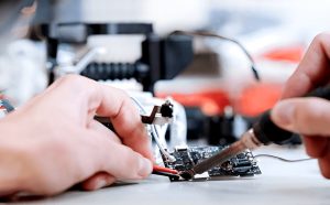
Soldering is the process that creates the permanent electrical and mechanical connection between a component and the PCB.
For SMT assemblies, reflow soldering is one of the most common methods. After solder paste printing and component placement, the populated PCB passes through a reflow oven. The board is heated through controlled temperature zones so that the solder melts and forms reliable solder joints before cooling and solidifying.
For through-hole assemblies, wave soldering or selective soldering may be used.
In wave soldering, the PCB is transported over a controlled wave of molten solder. The solder contacts the exposed through-hole leads and corresponding pads, forming solder joints as the board moves through the process.
Selective soldering is useful when only specific through-hole areas need to be soldered, particularly on mixed-technology boards containing both SMT and THT components.
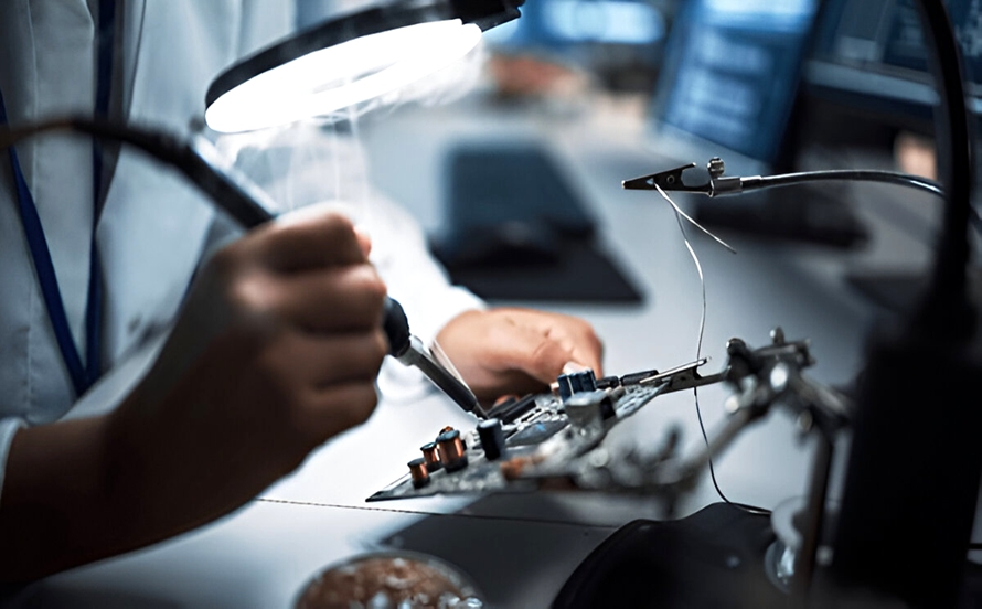
Manual soldering with a soldering iron may also be used for prototypes, low-volume production, repairs, modifications, or components that cannot be processed efficiently through automated soldering equipment.
A properly controlled soldering process should achieve:
- Adequate solder wetting
- Reliable electrical conductivity
- Appropriate solder joint geometry
- Sufficient mechanical strength
- Minimal solder bridging
- Minimal voiding where applicable
- No unintended short circuits
Soldering parameters must be matched to the solder alloy, PCB materials, component specifications, and assembly process rather than relying on a single universal temperature or time.
4. Testing and Verification of Component Connections
Inspection and testing should be performed throughout PCB Manufacturing and assembly rather than only after the finished board is completed.
During PCB design, engineers should verify the schematic, PCB layout, component footprints, BOM, and manufacturing constraints before releasing the design.
Incoming materials should also undergo appropriate quality inspection. Bare PCBs should be checked for manufacturing defects such as incorrect dimensions, damaged surfaces, drilling problems, opens, shorts, or other fabrication issues.
During assembly, component placement should be inspected to confirm:
- Correct component identity
- Correct position
- Correct orientation
- Correct polarity
- Proper alignment
- Proper solder coverage
Automated optical inspection (AOI) can help identify component placement and soldering defects, while X-ray inspection may be used for hidden solder joints such as certain bottom-terminated components and BGAs.
After assembly, electrical and functional testing can provide additional verification. Depending on the product, testing may include:
- Continuity testing
- Insulation or isolation testing
- In-circuit testing (ICT)
- Flying-probe testing
- Power-up testing
- Functional testing
- Communication interface testing
The appropriate testing strategy depends on the PCB design, production volume, circuit complexity, and product reliability requirements.
Key Points to Review When Connecting PCB Components
Several important factors should be reviewed throughout the component connection and assembly process:
- PCB Design: All components, footprints, nets, and reference designators should be accurately defined before manufacturing.
- Component Handling: Sensitive components should be stored and handled according to their ESD and moisture-sensitivity requirements.
- PCB Cleanliness: Flux residues and other contaminants should be managed according to the soldering process and product requirements.
- Flux Removal: When cleaning is required, an appropriate PCB cleaning method and compatible cleaning agent should be selected.
- Thermal Management: Heat-generating components should have sufficient copper area, thermal vias, heatsinks, or other appropriate thermal-management structures.
- Solder Joint Inspection: Solder joints should be inspected for defects such as bridges, insufficient solder, poor wetting, cracks, and component misalignment.
- Electrical Testing: The assembled PCB should be tested for unintended shorts, opens, incorrect connections, and functional failures.
- Manufacturing Documentation: BOM, fabrication data, assembly drawings, and other production files should remain consistent with the released PCB design.
These controls help reduce assembly defects and improve the repeatability and reliability of the final product.
PCB Design and PCB Manufacturing Must Work Together
Connecting components correctly is not only an assembly issue. It begins during PCB Design.
A PCB layout that does not consider manufacturing and assembly requirements can create significant problems later. For example, insufficient component spacing can make automated placement or inspection difficult. Inadequate solder-mask clearance can contribute to soldering problems, while poor thermal design can cause components to operate at excessive temperatures.
This is why Design for Manufacturing (DFM) and Design for Assembly (DFA) should be incorporated into the design process.
Engineers should communicate with the PCB manufacturer and assembler early enough to confirm important production requirements, including:
- Minimum trace width and spacing
- Minimum drill size
- Pad and annular-ring requirements
- Board thickness
- Copper thickness
- Surface finish
- Solder-mask clearance
- Component spacing
- Panelization requirements
- Assembly capabilities
- Inspection requirements
Exact manufacturing limits vary by supplier and process, so the manufacturer’s current capabilities should always be confirmed before the design is finalized.
Conclusion
Connecting electronic components to a PCB is one of the most important stages of PCB Assembly. Every component contributes to the overall electrical and functional performance of the finished product, and incorrect placement, orientation, polarity, or soldering can cause anything from intermittent faults to complete circuit failure.
A reliable component connection process starts with accurate PCB Design, continues through controlled PCB Manufacturing and component placement, and ends with appropriate inspection and electrical or functional testing.
By carefully managing component footprints, placement, soldering, cleanliness, thermal performance, and testing requirements, engineers and manufacturers can improve assembly quality and long-term PCB reliability. As electronic products continue to become smaller, more powerful, and more complex, efficient and precise component integration will remain a fundamental requirement for modern PCB manufacturing.