SMT PCB Assembly Process: PCB Design, PCB Manufacturing & SMT Guide
Surface Mount Technology (SMT) is one of the primary assembly methods used in modern custom PCB production. Compared with traditional through-hole assembly, SMT enables smaller component packages, higher component density, and highly automated production.
If you work with a contract manufacturer for custom electronics, your boards will often pass through an SMT production line, either as an SMT-only assembly or as part of a mixed-technology process that combines SMT and through-hole components.
Understanding the SMT PCB Assembly process can help you prepare more complete production documentation, identify potential design problems before manufacturing, and communicate more effectively with your manufacturing partner.
Step 1: Solder Paste Printing
The SMT process begins with applying solder paste to the pads of a bare PCB.
A stainless-steel stencil is aligned with the PCB so that its apertures correspond precisely to the required solder pads. A squeegee then moves across the stencil, forcing solder paste through the openings and depositing a controlled amount of solder paste onto each pad.
Solder paste volume, alignment, and consistency are critical to assembly quality. Too little solder paste can contribute to insufficient solder joints, while excessive paste can increase the risk of solder bridging, particularly on fine-pitch components.
Modern SMT production lines commonly use Solder Paste Inspection (SPI) after printing. SPI systems measure solder paste deposition and can identify problems such as insufficient or excessive paste volume, offset, and missing deposits before components are placed.
This early inspection is valuable because correcting a printing problem before placement and reflow can prevent an entire batch of boards from developing the same soldering defect.
Step 2: Automated Component Placement
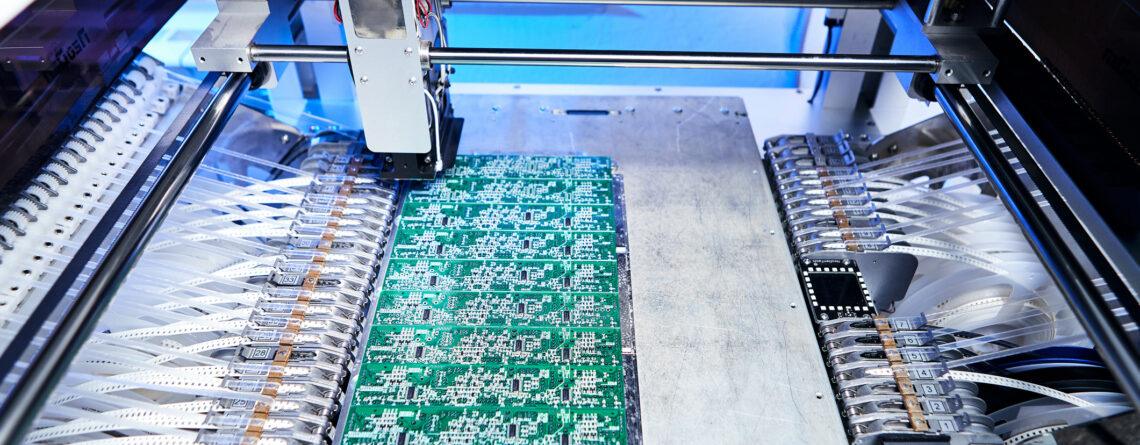
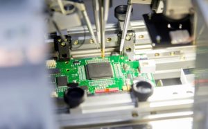
After solder paste printing, automated pick-and-place machines collect components from feeders, trays, or tubes and place them onto the corresponding PCB pads.
Modern placement equipment can handle a wide range of component packages, including:
- Small passive components such as resistors and capacitors
- QFP, QFN, and BGA integrated circuits
- Fine-pitch components requiring high placement accuracy
- Connectors and larger components compatible with the SMT process
- Specialized packages used in compact electronic products
The placement program is generated from production data such as the bill of materials (BOM), centroid or pick-and-place files, component libraries, and PCB design data.
Accurate placement data is essential. Errors in component coordinates, package orientation, polarity, or reference information can result in misplaced, missing, or incorrectly oriented components.
This is why accurate PCB Design documentation and a properly managed BOM are important before production begins.
Step 3: Reflow Soldering
Once the components have been placed, the PCB enters a reflow soldering oven.
The board passes through multiple controlled thermal zones. The temperature profile gradually heats the PCB and solder paste, reaches a temperature appropriate for the selected solder alloy, and then cools the assembly in a controlled manner.
During the process, the solder paste melts and wets the component terminals and PCB pads. As the assembly cools, the solder solidifies and forms the electrical and mechanical connections between the components and the board.
The reflow profile must be matched to the solder alloy, PCB construction, component thermal characteristics, and assembly requirements.
For lead-free production, for example, the thermal profile generally differs from that used for traditional leaded solder alloys. Large thermal-mass components and boards with significant variation in copper distribution may also require careful profile optimization.
Nitrogen-assisted reflow may be used for certain applications to reduce oxidation and improve process control, but whether it is necessary depends on the solder materials, components, PCB surface finish, and required quality level.
Step 4: Automated Optical Inspection (AOI)
After reflow soldering, the assembled PCB can undergo Automated Optical Inspection (AOI).
AOI systems use cameras and controlled lighting to inspect component presence, placement, solder joints, polarity markings, and other visible characteristics against predefined inspection criteria.
Typical defects that AOI may detect include:
- Missing components
- Incorrect component placement
- Component orientation or polarity errors
- Solder bridges
- Insufficient or excessive visible solder
- Misaligned components
- Certain solder-joint defects that are optically detectable
AOI is a non-destructive inspection method and can provide automated inspection coverage across the board. However, AOI cannot see every type of defect. For example, solder joints hidden underneath BGA packages generally require another inspection method, such as X-ray inspection.
Boards identified by AOI as potentially defective are normally reviewed according to the manufacturer’s inspection and disposition procedures.
Step 5: X-Ray Inspection for Hidden Solder Joints
Some component packages contain solder joints that cannot be directly inspected from the PCB surface.
BGA packages are a common example because the solder balls are located underneath the package body. Other bottom-terminated packages can present similar inspection challenges.
X-ray inspection provides a non-destructive method for examining hidden solder connections. Depending on the equipment and inspection requirements, it can help identify issues such as:
- Voids
- Bridging or solder shorts
- Missing solder connections
- Abnormal solder-ball formation
- Certain placement or soldering defects hidden from optical inspection
X-ray inspection can be particularly valuable for high-density assemblies, BGA-based designs, power electronics, and products with demanding reliability requirements.
However, X-ray inspection requirements should be determined based on the component types, product risk, customer specifications, and applicable quality standards rather than automatically applied to every PCB assembly.
Step 6: Through-Hole Components and Secondary Operations
Many custom PCB assemblies combine SMT with through-hole components.
Examples include:
- Board-to-board and wire-to-board connectors
- Large capacitors
- Transformers
- Relays
- Mechanically stressed components
- Other components specifically designed for through-hole mounting
Depending on the product design, through-hole components may be inserted before or after reflow, and the soldering method may include wave soldering, selective soldering, or manual soldering.
The exact sequence depends on component construction, solderability, thermal requirements, board design, and the selected manufacturing process.
After soldering, additional operations may include:
- Component lead trimming
- Manual rework
- Cleaning
- Conformal coating
- Programming
- Functional testing
- Mechanical assembly
- Enclosure or chassis integration
Not every PCB requires all of these operations. The process should be defined according to the product’s engineering and quality requirements.
Step 7: Final Inspection and Testing
After assembly and any required secondary operations, the PCBA may undergo additional inspection and testing.
Depending on the application, this can include:
Visual Inspection
Technicians or automated systems inspect the overall assembly for visible defects, contamination, damaged components, workmanship issues, and other abnormalities.
Electrical Testing
Testing may include methods such as:
- In-circuit testing (ICT)
- Flying-probe testing
- Continuity testing
- Insulation or isolation testing
- Functional testing
The appropriate test strategy depends on the complexity and quantity of the product, test-point accessibility, fixture requirements, and functional specifications.
Programming and Functional Verification
For programmable electronic products, firmware may be loaded onto the assembled board before final functional verification.
The PCBA can then be tested under defined operating conditions to verify that the assembled product performs according to its intended requirements.
What Does the SMT Process Mean for Your Custom PCB?
The SMT process is highly automated, but production quality depends heavily on the quality of the engineering data provided to the manufacturer.
Important inputs include:
- Clean and complete fabrication data
- Accurate BOM
- Correct pick-and-place files
- Verified component footprints
- Correct polarity and orientation information
- Appropriate PCB stackup
- Assembly drawings
- Test requirements
- Approved component specifications
For example, an incorrect footprint in the PCB Design can cause a component to sit incorrectly on the PCB even when the pick-and-place machine is operating properly.
Likewise, an inaccurate BOM can lead to incorrect components being purchased or loaded into the assembly line.
Therefore, successful PCB Manufacturing and PCB Assembly depend on consistency between the design data, fabrication data, component information, and assembly documentation.
Why DFM and DFA Reviews Matter
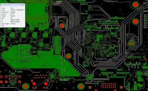
Design for Manufacturing (DFM) and Design for Assembly (DFA) reviews should ideally take place before production begins.
A professional review can identify potential problems such as:
- Insufficient component-to-component clearance
- Difficult-to-manufacture pad geometry
- Inappropriate solder mask openings
- Incorrect or inefficient component footprints
- Components positioned too close to the PCB edge
- Inaccessible test points
- Potential solder bridging risks
- Difficult-to-assemble connectors
- Thermal imbalance during reflow
- Conflicts between SMT and through-hole components
For high-density boards, these checks become increasingly important because small layout changes can significantly affect assembly yield.
A DFM/DFA review does not replace electrical design verification. Instead, it complements the engineering process by checking whether the design can be fabricated and assembled efficiently using the selected production process.
Common SMT Assembly Problems
Several common SMT defects can be traced to the interaction between PCB Design, materials, equipment, and process settings.
Solder Bridging
Excess solder paste, insufficient pad spacing, stencil design issues, or process variation can contribute to solder bridges between adjacent pads.
Tombstoning
A small passive component can stand on one end during reflow when uneven solder forces or thermal conditions affect the two terminals differently.
Component Misalignment
Incorrect placement data, component movement during reflow, or printing problems can result in component misalignment.
Insufficient Solder
Insufficient solder paste deposition or poor solder wetting can contribute to weak or incomplete solder joints.
Voids
Gas or flux-related voids can remain inside some solder joints after reflow. Their significance depends on the component, joint geometry, thermal requirements, and applicable acceptance criteria.
Missing Components
Feeder problems, incorrect setup, component shortages, or programming errors can result in missing components.
Effective SPI, AOI, X-ray inspection where appropriate, and functional testing can help detect different categories of defects throughout the production process.
How PCB Design Affects SMT Assembly
Good PCB Design is fundamental to reliable SMT production.
Engineers should consider assembly requirements while creating the layout rather than waiting until the board reaches the factory.
Important design considerations include:
- Component spacing
- Component orientation
- Pad geometry
- Footprint accuracy
- Solder mask design
- Stencil requirements
- Thermal relief
- Via placement
- Fiducials where required
- PCB edge clearance
- Test-point accessibility
- Panelization
- Component height and mechanical clearance
Component orientation can also influence automated assembly and inspection. Consistent orientation of similar components may simplify machine programming, inspection, and manual troubleshooting.
At the same time, the design must satisfy electrical requirements such as signal integrity, power distribution, thermal management, and electromagnetic compatibility.
The goal is not simply to make a PCB easy to assemble. The goal is to create a design that balances electrical performance, mechanical requirements, manufacturability, assembly efficiency, reliability, and cost.
SMT Assembly and PCB Manufacturing: How They Work Together
PCB Manufacturing creates the bare board that provides the electrical and mechanical foundation for the assembly process.
SMT assembly then uses that board to mount and solder electronic components.
The two processes are therefore closely connected.
For example, PCB manufacturing decisions involving:
- Board thickness
- Copper thickness
- Surface finish
- Solder mask
- Via structure
- Layer stackup
- Pad geometry
can directly affect SMT assembly.
Similarly, assembly requirements can influence the PCB design and fabrication process.
This is why an integrated review of PCB Design, PCB Manufacturing, and assembly requirements before production can reduce avoidable problems.
How Kingda Can Support SMT PCB Assembly
For custom electronics projects, Kingda can support a coordinated production workflow covering PCB fabrication and assembly requirements.
Depending on the project, the process can include engineering review, DFM/DFA analysis, PCB fabrication, component sourcing, SMT assembly, through-hole assembly, inspection, and testing.
The exact production flow should be determined by the board design, component mix, volume, reliability requirements, and customer specifications.
For engineering and purchasing teams, working with a coordinated manufacturing partner can reduce communication gaps between PCB fabrication and assembly and make it easier to address manufacturing issues before they become production problems.
Conclusion
The SMT PCB Assembly process combines precision printing, automated component placement, controlled reflow soldering, optical inspection, and, when required, X-ray inspection and additional assembly operations.
The basic workflow can be summarized as:
Solder Paste Printing → SPI → Component Placement → Reflow Soldering → AOI → X-Ray Inspection When Required → Through-Hole/Secondary Operations → Testing
The success of this process depends on more than advanced assembly equipment. Accurate BOMs, reliable pick-and-place data, correct footprints, suitable PCB materials, manufacturable layouts, and effective DFM/DFA reviews are equally important.
For custom electronics, integrating PCB Design, PCB Manufacturing, and SMT assembly considerations from the beginning can help reduce production problems, improve consistency, and create a smoother transition from prototype to volume production.