PCB Manufacturing vs. PCB Assembly: PCB Design, PCB Manufacturing & Custom PCB Guide
If you are purchasing a printed circuit board for the first time, you will quickly encounter two terms: PCB Manufacturing and PCB Assembly. Although they sound similar and are sometimes used interchangeably by suppliers, they refer to two different stages of the electronics production process.
Understanding the difference between PCB Manufacturing and PCB Assembly can help you ask better questions, prepare clearer specifications, compare supplier capabilities, and choose the right manufacturing partner for your project.
This guide explains what each process involves, where PCB fabrication ends and assembly begins, and why working with a supplier that can manage both processes can be particularly useful for custom electronics development.
What Is PCB Manufacturing?
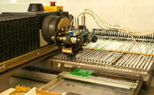
PCB Manufacturing is the process of fabricating a bare printed circuit board. At this stage, the board contains no electronic components and is not yet a functional electronic assembly.
The finished bare PCB provides the physical platform that supports the electrical connections between components. The manufacturing process starts with engineering and fabrication data, such as Gerber files, drill files, and stackup specifications, and ends with a bare board that meets the required layer count, materials, copper thickness, trace geometry, and surface-finish requirements.
Typical PCB Manufacturing steps include:
- Laminating copper-clad materials according to the required stackup
- Drilling through-holes, vias, and other required holes
- Creating copper circuitry through imaging and etching or other applicable processes
- Plating holes and copper features where required
- Applying solder mask and silkscreen
- Applying a surface finish to exposed copper pads, such as ENIG, HASL, immersion silver, immersion tin, or OSP
- Performing electrical and visual inspections
The result is a bare PCB that is ready to proceed to the assembly stage.
It is important to distinguish the PCB surface finish from the solder mask. The surface finish protects exposed copper pads and supports solderability, while the solder mask is the protective coating applied over areas that generally should not be soldered.
What Is Custom PCB Assembly?
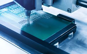
Custom PCB Assembly is the process of mounting electronic components onto a fabricated bare board and soldering them in place to create a functional PCBA.
This is the stage where the physical circuit board becomes an electronic assembly capable of performing its intended function.
Two major assembly technologies are commonly used.
Surface Mount Technology (SMT)
Surface Mount Technology (SMT) places components directly onto solder paste-covered pads on the PCB surface. The board then passes through a reflow soldering process, where the solder paste is heated according to a controlled thermal profile to form reliable solder joints.
SMT is widely used for compact electronics because it supports high component density and small packages.
Through-Hole Assembly
Through-hole assembly places component leads through holes drilled in the PCB. The leads are then soldered, commonly using wave soldering, selective soldering, or manual soldering, depending on the component mix and production requirements.
Through-hole technology remains useful for connectors, power components, mechanically stressed components, and other applications where through-hole construction provides practical benefits.
Mixed-Technology PCB Assembly
Many modern products combine SMT and through-hole components on the same board. This is known as mixed-technology assembly.
The appropriate process depends on the PCB Design, component package types, board construction, production volume, reliability requirements, and testing strategy.
What Happens Between PCB Manufacturing and PCB Assembly?
The simplest way to understand the relationship is:
PCB Manufacturing produces the bare board, while PCB Assembly turns that board into a functional electronic assembly.
In a typical production workflow, PCB Manufacturing comes first and PCB Assembly follows.
The fabrication stage creates the physical structure, including:
- Copper layers
- Dielectric materials
- Vias and plated holes
- Solder mask
- Silkscreen
- Surface-finished pads
The assembly stage then adds:
- Electronic components
- Solder joints
- Connectors and mechanical components where applicable
- Programming or configuration when required
- Inspection and functional testing
The output of PCB Manufacturing is therefore a bare PCB, while the output of PCB Assembly is generally referred to as a PCBA.
What Files Are Required for PCB Manufacturing and Assembly?
One of the most important differences between the two processes is the production data they require.
PCB Manufacturing Documentation
A fabricator commonly requires files such as:
- Gerber files
- NC drill files
- PCB stackup specifications
- Board dimensions and tolerances
- Copper thickness requirements
- Material specifications
- Surface-finish requirements
- Fabrication drawings when applicable
Gerber files primarily describe the artwork for the different PCB layers. They do not replace the complete set of assembly documentation.
PCB Assembly Documentation
An assembly supplier commonly requires:
- Bill of Materials (BOM)
- Pick-and-place / centroid files
- PCB layout or fabrication data
- Assembly drawings
- Component polarity and orientation information
- Assembly specifications
- Special process requirements
- Testing and programming requirements when applicable
The exact file package varies depending on the supplier and project.
Providing complete and consistent documentation reduces ambiguity and helps the manufacturer identify potential issues before production.
Why DFM Matters to Both Processes
Design for Manufacturing (DFM) is particularly important because PCB Design, PCB fabrication, and assembly are closely connected.
A design may be electrically correct but still create manufacturing difficulties.
For example, a design review may identify:
- Insufficient copper-to-edge clearance
- Trace or spacing dimensions that exceed the fabricator’s capabilities
- Inappropriate via structures
- Difficult-to-manufacture board thickness or stackup
- Insufficient component clearance
- Poor pad or footprint geometry
- Components that are difficult to place or solder
- Test points that are inaccessible
- Potential assembly conflicts between adjacent components
A DFM review before fabrication can address these issues while changes are still relatively inexpensive.
For custom PCB projects, this is particularly valuable because the board stackup, material selection, component package, routing density, and assembly process often need to be considered together.
Why Use One Supplier for PCB Manufacturing and Assembly?
Some companies purchase bare boards from one supplier and then send them to another company for PCB Assembly. This approach can work, particularly when procurement requirements or supplier specialization make it appropriate.
However, using a single supplier for both processes can simplify project management.
One Engineering Contact
Your engineering and purchasing teams can communicate with one supplier instead of coordinating fabrication and assembly separately.
Better Process Coordination
The fabricator and assembly team can coordinate material selection, board thickness, surface finish, component placement, soldering requirements, and testing requirements.
Earlier Problem Detection
If a fabrication feature creates an assembly problem, an integrated supplier may be able to identify the issue during engineering review rather than after boards have already been manufactured.
Fewer Logistics Handoffs
When bare boards and assembly are managed through the same supplier, the project can avoid unnecessary transportation and supplier-to-supplier handoffs.
Simplified Quality Management
When a defect is discovered, it can be easier to trace the issue across fabrication, assembly, inspection, and testing when these processes are managed within one coordinated production workflow.
This does not mean that a single supplier is always the right choice. Supplier selection should depend on technical capability, quality requirements, capacity, lead time, cost, communication, and the specific needs of the project.
PCB Manufacturing vs. PCB Assembly: Key Differences
| Factor | PCB Manufacturing | PCB Assembly |
|---|---|---|
| Main purpose | Fabricate the bare circuit board | Install and solder electronic components |
| Main output | Bare PCB | Assembled PCBA |
| Major inputs | Gerber, drill, stackup, fabrication specifications | BOM, placement data, assembly drawings, PCB data |
| Main processes | Imaging, etching, drilling, plating, lamination, solder mask, surface finishing | SMT, through-hole assembly, soldering, inspection, testing |
| Components installed? | No | Yes |
| Functional electronics? | No | Generally yes, after required testing |
| Key considerations | Layer structure, materials, copper, vias, tolerances, surface finish | Components, footprints, soldering, placement, inspection, testing |
| Main quality concerns | Open/short circuits, dimensional accuracy, layer registration, plating, surface finish | Solder defects, component placement, polarity, missing parts, assembly quality |
How PCB Design Affects Both Processes
A successful project starts with a manufacturable and assemblable PCB Design.
During the design stage, engineers should consider both fabrication and assembly requirements rather than treating them as completely separate problems.
Important considerations include:
- Board dimensions and tolerances
- Layer count and stackup
- Material selection
- Copper thickness
- Trace width and spacing
- Via structure
- Controlled impedance requirements
- Component footprints
- Component spacing
- Solder mask clearances
- Surface finish
- Thermal management
- Test-point accessibility
- Assembly orientation
- Manufacturing panelization
For example, selecting a very small component package may help reduce board size, but it can also introduce more demanding assembly requirements. Similarly, a dense routing structure may achieve the desired electrical performance but require a more advanced fabrication process.
Therefore, PCB Design should be developed with the intended PCB Manufacturing and assembly capabilities in mind.
Common Mistakes When Ordering PCB Manufacturing and Assembly
Treating PCB Fabrication and Assembly as the Same Process
A bare PCB is not the same as an assembled PCBA. Each stage has different equipment, documentation, process controls, and quality requirements.
Providing Incomplete Production Data
Missing Gerber layers, drill information, BOM data, placement files, or assembly drawings can delay engineering review and production.
Ignoring DFM and DFA
DFM focuses on manufacturing feasibility, while Design for Assembly (DFA) considers how efficiently and reliably components can be assembled.
Both should be considered before production.
Selecting Components Without Considering Assembly
A component may meet the electrical specification but still present sourcing, placement, soldering, inspection, or testing challenges.
Assuming Every Supplier Has the Same Capabilities
PCB manufacturers and assembly providers have different equipment, minimum feature capabilities, materials, package support, testing methods, and production limits. Always confirm the supplier’s current capabilities before finalizing the design.
How Kingda Can Support Custom PCB Projects
For custom electronics, coordinating PCB Manufacturing and PCB Assembly through one experienced production partner can simplify communication and improve process continuity.
Kingda can be positioned as a single manufacturing partner for projects that require coordination between bare-board fabrication and assembly. Depending on project requirements, the workflow can include engineering review, PCB fabrication, component sourcing, SMT and through-hole assembly, inspection, and testing.
For engineering and purchasing teams, the key advantage of an integrated workflow is not simply having fewer suppliers. It is the ability to coordinate the entire production chain around the same technical requirements.
Conclusion
PCB Manufacturing and PCB Assembly are two separate but closely connected stages of electronics production.
PCB Manufacturing creates the bare circuit board by building the required copper layers, dielectric structure, vias, solder mask, silkscreen, and surface finish. PCB Assembly then installs and solders electronic components onto that board to create a functional PCBA.
The distinction also affects the documentation required for production. Fabrication generally relies on Gerber, drill, stackup, and manufacturing specifications, while assembly additionally requires information such as the BOM, pick-and-place data, and assembly drawings.
For custom electronics, considering fabrication and assembly together during PCB Design can reduce avoidable manufacturing problems and improve production coordination. Whether you use one supplier or multiple specialized suppliers, the most important factors are technical capability, quality control, communication, cost, lead time, and the requirements of your specific product.
For projects that require both PCB Manufacturing and assembly, an integrated manufacturing workflow can provide a practical way to manage engineering review, fabrication, assembly, inspection, and testing from a coordinated production process.