Adding a Logo on a PCB: Silkscreen Versus Copper Artwork
A logo or a marking on a board is a small feature with a surprising number of ways to go wrong. It shares space with pads and vias, it has to survive the assembly process, and it has to be legible on a board that may be only a few millimetres wider than the part it is printed beside. Getting a logo onto a board is easy; getting it onto a board so that it looks deliberate and does not affect the build is a short series of decisions.
What a Board Marking Is For
Not every marking is decoration. A company identification or a model number on the silkscreen helps a technician identify a board that is already installed. A revision letter is the cheapest way to prevent a service centre from fitting the wrong assembly. A pin-one marker, a polarity bar or a connector label is functional, and its absence causes assembly errors that no test can catch. A QR or Data Matrix code printed on the board is increasingly used to tie a physical unit to its test record, which is only useful if the code stays readable after reflow.
Deciding which of these the board needs comes first, because the answer determines where the marking goes and how much space it can occupy.
Preparing the Artwork
The artwork itself has to be a monochrome bitmap, one bit per pixel, with no grey. A photograph or a screenshot cannot be placed directly: the greys would have to become either solid or absent, and the algorithm that does that decides how the logo looks.
The steps are the same in any tool. Convert the image to a single-bit image and set the threshold by eye, because the threshold is what preserves the thin strokes of a letter or the fine detail of a symbol. Scale the image to the size it will occupy on the board and re-examine it, since a bitmap that was prepared at a large size may lose its detail when it is reduced. Clean up the stray pixels that the conversion leaves behind, because each one becomes a copper or ink feature at the resolution of the artwork.
Where the source graphic is a vector file, it is worth keeping it in vector form and converting to a polygon region rather than to pixels, because the result has smooth curves that do not depend on a pixel grid. The trade-off is that small text converted from a bitmap can come out sharper at the board”s printing resolution than the same text converted from a low-resolution vector trace.
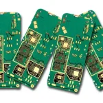
<img src="https://www.gopcba.com/wp-content/uploads/2026/06/汽车电子PCBA图.jpg" alt="logo prepared as a monochrome bitmap for a PCB” />
Two Ways to Render the Marking
A logo on a PCB can be produced in one of two materials, and the choice changes everything about the design.
Printed in the silkscreen, the marking is non-conductive ink applied on top of the solder mask. It costs nothing in copper and it has no electrical consequence at all. Its limits are process limits: the ink has a minimum line width, and it does not print reliably across a surface that is not flat, which is why silkscreen over a via or over a pad is either clipped by the designer or removed by the fabricator. Fine detail is possible but is limited by the screen printing resolution, so a logo with hairline strokes should be redrawn with thicker ones.
Rendered in copper, the marking is etched from the same layers as the circuits. Copper can hold finer detail than silkscreen and it cannot wear off, and a copper feature can be left exposed by opening the solder mask over it, which is how gold or bare copper branding appears on a board. Exposed copper carries a caveat: a large exposed area of copper on a surface that will be soldered nearby can attract solder, and the surface finish has to be compatible with the process.
A copper logo can also be left covered by the solder mask, which produces a subtle marking visible as a change in surface height. This is the most robust option, because nothing can wear off and nothing can be wetted, and it is what many industrial products use.
Placement Rules That Matter
The marking has to live inside the rules that govern everything else on the board.
Keep it clear of pads and of solder mask openings. Silkscreen that overlaps a pad opening is removed or clipped by the fabricator, and a logo that depends on a clipped edge looks broken.
Keep it away from the board edge by the same margin used for the copper, because a marked feature that reaches the routed edge is cut away when the panel is depanelised.
Do not place it on a breakaway tab or on the rail. The marking disappears with the tab, and the tab is where the customer least expects to lose information.
Check the orientation of the text when the board is viewed from the assembled side. A marking that is readable when the board is flat on a bench may be hidden by a connector or a shield can once the assembly is complete, and the practical convention is to orient the marking so that it reads from the same direction as the reference designators.
For a logo placed on the bottom layer, mirror the artwork. A marking transferred without mirroring is correct on the screen and reversed on the finished board, and this error is only visible in the physical item.

When the Marking Has to Be on Copper
Copper markings deserve one extra check, because they interact with the electrical design. A large solid copper logo has to be isolated from every net, which means a clearance region around it, and that region has to be respected by the copper fill rather than filled back in. An isolated copper island also has to be connected or it becomes floating copper, which is generally avoided because it can act as a patch antenna; connecting it to ground through a small feature resolves it.
The etch process is another factor. A large area of copper with fine detail inside it etches unevenly, because the etchant has to travel further to reach the middle of the region. The effect can be reduced by hatching the logo, by keeping the solid areas modest, and by placing the logo where the surrounding copper density is similar. These are the same considerations that apply to any large copper area, and they belong in the data review rather than in a post-mortem. Our PCB manufacturing team checks the artwork for them with the rest of the design.
Checking the Result
The reason to place a marking is that it will be read later, and the only way to know that it will be readable is to look at it as it will be produced. Print the silkscreen layer alone at the size of the printed board, or view the copper artwork with the fill and the mask removed. If the text is uncertain at that stage, it will be worse on the finished board.
For a service record, a readable marking inside the board outline is worth more than a logo on the edge of the panel. Our quality management flow ties the board revision to the build record, and our layout support can place the marking along with the rest of the documentation features so that a revision letter is never missing from a board.
FAQ
Can any image be used as a logo? Only after it is converted to a single-bit image at the final size and cleaned of stray pixels. The conversion threshold changes how the logo looks, so it should be checked on a printout.
Is copper better than silkscreen for a logo? Copper holds finer detail and cannot wear off. Silkscreen costs nothing in copper and has no electrical consequence. The choice depends on whether the marking must survive handling and abrasion.
Why did my logo disappear on the finished boards? The usual causes are printing over a pad or a mask opening, placing the marking on a breakaway tab, or reaching the routed edge.