Analog and Digital Circuits: Where the Difference Shows Up in Layout
The usual summary is that digital circuits handle zeros and ones while analogue circuits handle continuously varying signals. That is true and it stops well short of anything useful. The difference that matters on a board is not the shape of the signal but what the two kinds of circuit need from their environment: how much noise they tolerate, how they return current, and what happens where they meet.
Almost every product contains both, and the boundary between them is where most of the difficult problems live. A sensor output is analogue, a converter digitises it, a processor handles the result, and a driver may convert it back to an analogue quantity such as a motor current or a display voltage.
What Each Domain Actually Is
An analogue circuit processes a quantity that is continuous in time and amplitude: the voltage from a thermocouple, the output of a microphone, the current through a shunt. Every physical measurement begins as an analogue signal, which makes analogue design the bridge between the physical world and everything that follows.
A digital circuit works with discrete states and defined thresholds. Its advantages are noise immunity, straightforward storage and processing, and a design methodology that can be standardised and verified with tools. The immunity is real, but it is bounded: a digital input ignores noise until the noise is large enough to cross the threshold, and then it does not ignore it at all.

Noise Margin and What It Means for Layout
A digital input has a defined margin between the guaranteed output level of the driver and the threshold of the receiver. That margin is the space in which noise is allowed to exist. Analogue circuits have no equivalent binary threshold; any disturbance appears directly in the signal, and its importance depends on the resolution of the system that reads it.
The practical consequence is that the same interference can be harmless in one part of the board and fatal in another. A few tens of millivolts of ground noise is irrelevant to a digital bus with half a volt of margin and is a large error at a precision analogue input whose full scale is measured in millivolts. This is why the analogue and digital sections are separated, and it is also why a separation that is only written on the schematic achieves nothing.
Grounding and Return Paths
Digital circuits return current in short, high rate pulses. The return path therefore has to be continuous and low in inductance, because the current follows the path of least impedance, which at high frequency means the path directly beneath the trace.
Analogue circuits are more concerned with the potential of the reference itself. If a sensitive amplifier shares a return segment with a switching digital load, the local ground potential moves with the digital current, and the amplifier sees that movement as part of its input. The classic remedy is to partition the return paths so that the noisy currents do not flow through the reference used by the sensitive circuit, while keeping a single reference plane where the two sections meet so that no trace has to cross a split.
The reason a split plane is dangerous is worth stating plainly: a signal that crosses a gap in its reference plane has no adjacent return path, so its return current takes a long detour, which enlarges the loop and increases both emissions and coupling. Partitioning should be done by placing the circuits so that the currents separate naturally, not by cutting the plane under the signals. A ground partition is a layout of currents, not an absence of copper.
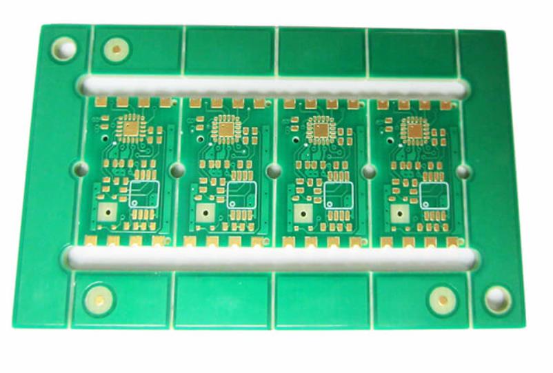
<img src="https://www.gopcba.com/wp-content/uploads/2026/08/Automatic-PCBA-Cleaning.webp" alt="converter interface grounding” />
Where the Two Domains Meet
The interface between them is the converter, and it deserves its own design review. The analogue input needs its filtering and its reference to be quiet, and the digital output switches current into the same package. The reference, the supply decoupling and the placement of the return connections determine whether the converter meets the resolution its datasheet promises or delivers something considerably worse.
The layout decisions are specific. Keep the analogue input network close to the converter pins and away from the digital lines, return the analogue ground of the converter to the analogue reference rather than to the digital one, and keep the clock and data outputs routed away from the analogue input. Where the converter is a successive approximation type, the reference input is effectively a dynamic load and needs its own decoupling close to the pin.
Design Practice in Each Domain
Analogue work rewards understanding of device characteristics, noise, offset, drift and frequency response, and it is usually evaluated by measurement because the interactions are hard to predict from a schematic alone. Digital work rewards a systematic approach: timing analysis, signal integrity, protocol compliance and a verification plan that can be automated. Neither is a superset of the other, and a design that contains both needs both sets of habits.
The skills overlap more than the job titles suggest. An engineer working on power supplies is dealing with loop stability and with switching noise that couples into everything else, which is analogue work with a digital problem attached. An engineer working on a high speed interface is dealing with transmission lines and return paths, which is analogue reasoning applied to signals that happen to be binary.
Reviewing a Mixed Signal Board
The review is easier if it is split along the same boundary the circuit uses. On the analogue side, confirm that the input network is close to the amplifier or converter, that the reference is quiet and decoupled at the pin, and that the return has not been shared with anything that switches. On the digital side, confirm the impedance and the reference continuity, and check that no fast net has been routed across the analogue region for convenience.
At the boundary itself, identify every place a digital signal crosses into the analogue domain and confirm it is necessary. A layout review that treats the board as one electrical object rather than two will miss the interactions that only appear when the digital load switches, and those interactions are the ones that are expensive to diagnose later.
Once the board exists, the test plan should confirm what the layout assumed: measure the analogue input with the digital section idle and again while it is running at full activity, and compare the two results. A resolution figure quoted from a datasheet means very little until it has been measured under the conditions the product will actually experience. The same applies to the analogue components themselves, whose tolerance and temperature behaviour belong in the component selection for the design rather than in a general note.
FAQ
Can analogue and digital circuits share a ground plane? They normally should share one continuous reference, with the circuits arranged so that the return currents stay in their own regions rather than being forced to mix.
Why is analogue design considered harder to learn? Because the behaviour depends on many continuous parameters and on layout parasitics, and the results are often judged by measurement rather than by a pass or fail rule.
Do digital circuits need decoupling too? Yes, and for the same reason: the switching current has to be supplied locally so that it does not disturb the reference used by other circuits.
What is the most common mistake at the boundary? Routing a fast digital trace through the analogue section, or placing a converter so that its analogue and digital returns share the same impedance.
Summary
Analog and digital circuits are distinguished less by their signals than by what they require: a noise margin or a clean reference, a low inductance return or a stable potential, a verification method or a measured result. The board is where those requirements meet, and the boundary between the two domains is where a design either respects them or quietly ignores them.