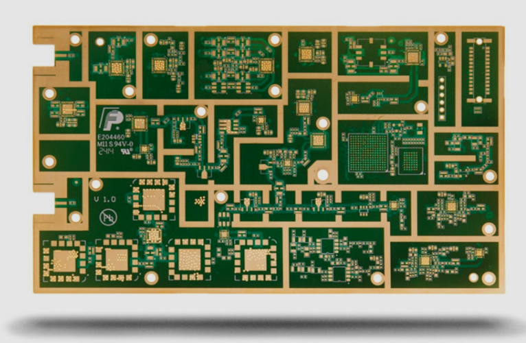
Analog Design Questions That Reveal Board Level Mistakes
Analog questions are useful in a design review because the answers reveal whether a team understands the board or only the schematic. A circuit that simulates perfectly can fail on a board because of a ground return, a decoupling assumption or a clock that was routed for convenience, and the fastest way to find those assumptions is to ask the questions that expose them.
What an Op Amp Datasheet Does Not Tell You
An op amp model describes the device, not the circuit it sits in. Input bias current, offset voltage and open-loop gain are all specified with an ideal supply and an ideal load, while the board supplies neither. The result is that a circuit whose gain error was calculated from the datasheet can measure noticeably worse once the feedback network, the source impedance and the supply impedance are real.
The question worth asking in review is what the source impedance is and how it interacts with the bias current. A high-impedance source turns a tiny bias current into an offset, and the fix is often a resistor of the matching value rather than a better op amp. Understanding the mechanism matters more than upgrading the part.
Grounding and the Return Path
Grounding is the topic where good engineers disagree most, because a rule that works in one design fails in another. The physical fact underneath the disagreement is that return current follows the path of least impedance, which for high frequencies means the path directly under the trace. Any layout that forces the current somewhere else creates a loop, and the loop is what couples into the analogue signal.
A practical review question is whether any sensitive analogue trace crosses a break in its reference plane. If the answer is yes, the fix is geometric rather than electrical, and no amount of filtering will restore the lost margin. Our notes on power plane splitting rules describe when a split helps and when it merely relocates the return current.

Clock Jitter and Mixed Signal Layout
Clock jitter is a system property, not a component parameter. It depends on the oscillator, on the buffer stages, on the supply noise that reaches them and on the return path under the clock net. Two boards with the same bill of materials can show different jitter because one of them routed the clock across a plane boundary or placed a switching regulator next to the clock buffer.
Mixed signal layout is where this becomes visible, because the analogue section measures small signals while the digital section generates large transient currents nearby. The review question is where those two domains meet and what separates them. A single continuous ground with a careful floorplan usually outperforms a split ground that forces return currents to take a long detour.
Decoupling Assumptions
Decoupling capacitors are chosen for their value and placed for their geometry, and the geometry usually decides the outcome. A capacitor placed a few millimetres from the pin, with its return path looping around the package, has an inductance that dominates its capacitance above a few megahertz. The question to ask is not what the value is but where the loop is.
The same reasoning explains why a large capacitor does not solve a high-frequency problem. Above the self-resonant frequency the part behaves as an inductor, so the useful work is done by several small capacitors with short connections rather than by one large one. Our notes on DC-DC converter layout and routing show the same principle applied to a switching supply.
Supply Noise That Reaches the Analogue Front End
Power supply noise reaches an analogue circuit through several paths at once: conducted along the rail, coupled through shared impedance and radiated from nearby switching nodes. Filtering one path while leaving the others open gives an improvement that disappears as soon as the operating conditions change, which is why the review question is about all the paths rather than about the filter.
The most common oversight is a shared return. When a sensitive amplifier and a switching stage return through the same piece of copper, the voltage developed across that copper appears in series with the analogue signal. Separating the returns until a single defined point is the standard remedy, and it has to be planned rather than added later.
Questions Worth Asking Every Time
Five questions cover most of the analogue risk on a mixed design. What is the source impedance at each input. Where does each return current flow. How much jitter does the clock path add. Which supply noise reaches the front end and by what path. What changes if the temperature moves by forty degrees. The answers are rarely perfect, but they are specific.
Our notes on EMI suppression design principles describe how the same loop-area reasoning applies to emissions, which is convenient because a board that answers these questions well tends to pass its EMC tests without heroics. The two problems share a cause even when they are measured differently.
What to Do With the Answers
The purpose of the questions is to convert a vague concern into a specific risk. If the source impedance is high and the bias current is large, the answer is a specific resistor. If the return path crosses a split, the answer is a specific reroute. Vague concerns produce general anxiety; specific risks produce changes to the layout while the layout is still editable.
That is why the review should happen on the floorplan and again after routing, with the same questions asked both times. At gopcb, analogue and mixed signal boards are reviewed with the ground and return structure drawn explicitly, so that the answers are visible on the drawing instead of being asserted in a meeting.
Additional Considerations for This Build
Practical attention to analog design questions pays for itself here, because it decides whether the finished board behaves as the drawing intended. Where the requirement is not stated on the fabrication drawing or in the assembly notes, the shop has to assume a default, and that default is rarely the value the design was simulated with. Stating analog design questions explicitly, together with the tolerance that applies, removes the assumption and keeps the result predictable from batch to batch.
Process Control and Verification
Reviewing the design before the data is released is far cheaper than correcting it after the panel is in the tank, because every step downstream inherits the decision made at the front end. Where a value sits close to a process limit, the drawing should say so, since the shop can then open the process window rather than working to a nominal figure that carries no tolerance.
The measurements that matter are the repeatable ones: conductor width and spacing, annular ring, finished hole size, plating thickness and surface finish are all verifiable on a coupon that travels with the panel. Documenting the assumption is part of the design work, and a short note on the drawing prevents a question that would otherwise arrive a day later and cost a day of schedule.
FAQ
Should analogue and digital grounds be separated? Usually not into two planes. A single continuous reference with a careful floorplan keeps return currents short. Separation helps only when specific currents must be kept apart, and then the join has to be planned.
Is a better op amp a substitute for layout discipline? No. A lower offset device reduces one error term while the return path and the decoupling loop continue to dominate the measured result. Layout comes first, then component selection.
How do I know whether jitter is a problem? Compare the measured jitter with the timing budget of the interface it clocks. If the margin is comfortable, further work is unnecessary; if it is thin, trace the supply and return path before changing the oscillator.