Back Drill PCB: PCB Design, PCB Manufacturing & Back Drilling Process
As the demand for higher data rates, improved signal integrity, and stricter electromagnetic interference/electromagnetic compatibility (EMI/EMC) performance continues to increase, printed circuit boards (PCBs) are becoming more complex. High-speed digital systems, networking equipment, servers, telecommunications devices, and other advanced electronics require PCB designs capable of maintaining stable electrical performance at increasingly high frequencies.
To address these challenges, engineers and PCB manufacturers use various techniques throughout the PCB design, fabrication, and assembly processes. One of these techniques is back drilling, which selectively removes unwanted via stubs that can negatively affect high-speed signal transmission.
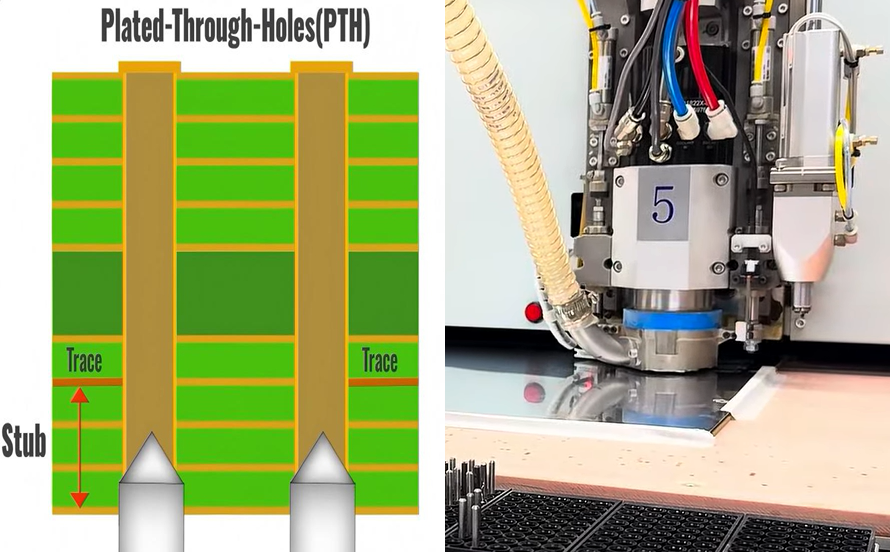
In a multilayer PCB stackup, a conventional through-hole via may extend through multiple layers even when the signal only needs to travel between a few of them. The unused portion of the via becomes a via stub. Although this unused section does not contribute to the intended electrical connection, it can introduce impedance discontinuities, signal reflections, resonances, insertion loss, and additional electromagnetic coupling at high frequencies.
This article explains what a Back Drill PCB is, why back drilling is important, how the back-drilling process works, key design parameters, common manufacturing problems, and best practices for implementing back drilling.
What Is a Back Drill PCB?
Back drilling is a controlled-depth drilling process used to remove the unused portion of a plated through-hole via after the conventional via has been fabricated.
Instead of drilling completely through the PCB again, a larger-diameter drill is used from the appropriate side of the board to remove the unwanted portion of the via barrel. The drilling depth is carefully controlled so that the drill stops before reaching the active signal layer.
The remaining via section provides the required electrical connection, while the unnecessary via stub is removed.
A simplified structure can be represented as:
Active Signal Layer → Required Via Connection → Back-Drilled Section → Removed Via Stub
The objective is not to remove the entire via, but to eliminate the portion that could interfere with high-speed signal transmission.
By reducing via-stub length, Back Drill PCB technology can reduce impedance discontinuities and unwanted signal reflections, helping improve signal integrity in demanding high-speed applications.
Why Is Back Drilling Important in PCB Design?
Back drilling becomes increasingly important as signal frequencies and data rates rise.
At relatively low frequencies, a small via stub may have little practical effect on circuit performance. However, as edge rates become faster and the electrical length of the stub becomes significant relative to the signal wavelength, the stub can behave as a transmission-line discontinuity.
This can result in:
- Signal reflections
- Impedance discontinuities
- Insertion loss
- Return loss
- Resonance
- Crosstalk
- Increased electromagnetic radiation
- Reduced signal integrity
- Eye-diagram degradation
For high-speed PCB design, controlling these effects can be essential.
Improved Signal Integrity
A long via stub creates an additional electrical structure that the signal can interact with.
Removing unnecessary via length reduces the discontinuity and provides a smoother transition between PCB layers.
This can improve signal quality, particularly in high-speed serial interfaces.
Reduced Impedance Discontinuity
Controlled-impedance routing requires consistent transmission-line geometry.
A via and its unused stub can introduce an impedance discontinuity. Back drilling shortens the unwanted structure and helps reduce this discontinuity.
Reduced EMI and Crosstalk
Unwanted via structures can contribute to electromagnetic coupling and resonance.
Reducing unnecessary conductive structures can help minimize certain EMI and crosstalk mechanisms, although the overall EMI/EMC performance still depends on the complete PCB stackup, routing, grounding, shielding, and enclosure design.
Better High-Speed Performance
Back drilling is commonly considered for demanding high-speed PCB applications, particularly when conventional through-hole vias would create excessive stub length.
Typical applications include:
- High-speed servers
- Data-center equipment
- Network switches
- Telecommunications equipment
- High-performance computing systems
- High-speed industrial electronics
- Advanced computing hardware
However, not every PCB requires back drilling. The need should be determined by signal-integrity analysis and the electrical length of the via structure relative to the application’s operating frequency and edge rate.
Back Drilling Process in PCB Manufacturing
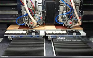
Back drilling is generally performed as a secondary drilling operation after the conventional through-hole has been drilled and plated.
The exact sequence depends on the manufacturer’s process and stackup, but a typical PCB Manufacturing workflow includes the following steps.
1. Through-Hole Drilling and Plating
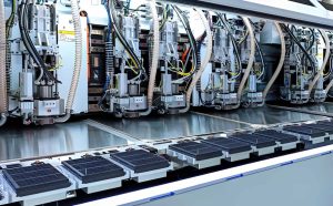
During conventional PCB fabrication, the required through-holes are drilled through the multilayer board.
The holes are then metallized through electroless copper deposition and subsequent copper plating to create conductive connections between the required layers.
At this stage, the plated through-hole may still extend through portions of the PCB that are electrically unnecessary.
2. Controlled-Depth Back Drilling
After the required through-hole fabrication steps, a larger drill is used from the appropriate side of the PCB.
The drill removes the unused portion of the plated via barrel.
The drilling depth must be carefully controlled so that the drill stops before reaching the active signal layer or another structure that must remain intact.
The required residual stub is therefore minimized without compromising the intended electrical connection.
3. Via Stub Removal
The primary objective of the operation is to remove as much unnecessary via stub as practical while maintaining the required connection.
The amount of residual stub depends on factors such as:
- PCB thickness
- Stackup configuration
- Signal-layer location
- Back-drill depth
- Drill diameter
- Manufacturing tolerance
- Registration accuracy
- Material characteristics
The manufacturer must establish appropriate back-drill parameters based on the PCB stackup and design requirements.
4. Cleaning and Inspection
After back drilling, debris generated during the drilling operation must be removed.
The PCB can then undergo inspection to verify drilling accuracy and overall board quality.
Depending on the design and quality requirements, inspection methods may include:
- Optical inspection
- Dimensional inspection
- Cross-sectional analysis
- X-ray inspection
- Electrical testing
- TDR measurements
Cross-section analysis is particularly useful for directly examining the back-drilled structure and measuring the remaining stub.
5. Final PCB Processing
After successful back drilling and inspection, the PCB continues through the remaining manufacturing operations as required.
These may include:
- Solder mask application
- Surface finishing
- Silkscreen printing
- Electrical testing
- Final inspection
- Packaging
The completed board can then proceed to PCB Assembly and system integration.
Key Back Drilling Parameters
Successful back drilling requires accurate control of several parameters.
Back-Drill Depth
Back-drill depth is one of the most critical parameters.
The drilling depth must be sufficient to remove the unwanted via stub while avoiding damage to the active signal layer.
The actual manufacturing tolerance should be defined with the PCB manufacturer because achievable accuracy depends on equipment, board construction, tooling, and process capability.
Back-Drill Diameter
The back-drill diameter is generally larger than the original finished via-hole diameter.
It must be large enough to remove the plated barrel section while maintaining sufficient clearance from nearby copper structures.
Residual Stub Length
The remaining via stub after back drilling is called the residual stub.
The shorter the residual stub, the less electrical discontinuity it generally introduces. However, the acceptable residual length depends on the application’s signal characteristics and design requirements.
Stackup
The PCB layer stackup determines where the active signal layers are located and therefore strongly affects the back-drill strategy.
A well-designed stackup can sometimes reduce the need for extensive back drilling.
Material Selection
PCB laminate properties can affect drilling performance and overall high-speed electrical behavior.
High-speed PCB designs may use specialized low-loss materials when required by the application.
The mechanical drilling process must also be matched to the material characteristics to prevent excessive tool wear, delamination, or other manufacturing defects.
Back Drill PCB Design Considerations
Back drilling should be considered during the PCB Design stage rather than being added after the layout has been completed.
Plan Back Drilling During Stackup Design
Engineers should determine which signal layers require high-speed transitions and identify vias that may create problematic stubs.
The stackup can then be optimized to minimize unnecessary via length.
Use Appropriate Via Structures
Not every high-speed connection requires back drilling.
Depending on the design, engineers may use:
- Blind vias
- Buried vias
- Microvias
- Through-hole vias
- Back-drilled vias
The appropriate structure depends on electrical requirements, manufacturing capabilities, board thickness, cost, and reliability requirements.
Maintain Controlled Impedance
High-speed traces should be designed with appropriate impedance targets.
The trace width, dielectric thickness, copper thickness, material properties, via geometry, and reference planes all contribute to impedance.
Back drilling should therefore be evaluated as part of the complete controlled-impedance design rather than as an isolated manufacturing operation.
Preserve Ground Return Paths
A high-speed signal requires an appropriate return-current path.
Back drilling cannot compensate for a poorly designed reference-plane structure.
Engineers should ensure that high-speed traces have continuous reference planes and that transitions between layers do not create unnecessary return-path discontinuities.
Consider Differential Pair Geometry
For high-speed differential signals, both traces should maintain appropriate geometry, spacing, coupling, and length relationships.
Via structures should be designed consistently across the differential pair.
If one side of a differential pair has significantly different via geometry from the other, the resulting asymmetry can affect differential signal performance.
Back Drilling Best Practices
Several practices can improve the effectiveness and manufacturability of a Back Drill PCB.
1. Plan Back Drilling Early
Back drilling should be incorporated into the PCB design process from the beginning.
Manufacturing documentation should clearly specify:
- Back-drill locations
- Back-drill diameter
- Back-drill depth
- Layer information
- Residual stub requirements
- Stackup information
- Manufacturing tolerances
- Special drilling instructions
Clear documentation helps prevent misunderstandings between the PCB designer and manufacturer.
2. Use Simulation Before Manufacturing
High-speed simulation can help determine whether a via stub is electrically significant.
Engineers can evaluate:
- S-parameters
- Insertion loss
- Return loss
- Impedance
- Reflection
- Crosstalk
- Eye diagrams
Simulation can help determine whether back drilling is necessary and how much stub reduction is required.
3. Optimize the Stackup
A carefully designed multilayer stackup can reduce the number of unnecessarily long vias.
In some cases, moving high-speed signal layers closer to the outer layers or using appropriate blind/buried via structures can reduce the need for back drilling.
4. Verify the Manufactured PCB
Simulation alone cannot guarantee manufacturing accuracy.
Physical verification can include:
- Cross-sectional analysis
- TDR testing
- Electrical testing
- Dimensional inspection
TDR can be particularly useful for identifying impedance discontinuities and evaluating high-speed interconnect structures.
5. Work With a Capable PCB Manufacturer
Back drilling requires specialized equipment and process control.
Before releasing a design for production, engineers should confirm that the selected PCB Manufacturing partner can meet the required:
- Back-drilling accuracy
- Hole-size tolerance
- Registration accuracy
- Residual-stub requirements
- Material compatibility
- Inspection requirements
This is especially important for high-speed and high-density multilayer PCBs.
Common Back Drilling Problems and Solutions
Although back drilling can improve high-speed PCB performance, incorrect design or manufacturing parameters can create new problems.
Problem 1: Incorrect Residual Stub Length
One common problem is incorrectly calculating or controlling the remaining stub length.
If too much of the via remains, the intended signal-integrity improvement may not be achieved.
If the drill penetrates too deeply, it may damage an active signal layer or compromise the via connection.
Solution:
Use accurate stackup data, carefully calculate the required drilling depth, and define appropriate manufacturing tolerances.
Cross-section verification can then confirm whether the manufactured residual stub meets the design requirements.
Problem 2: Excessive Drill Depth
Over-drilling can damage electrically active structures beneath the intended drilling depth.
This can cause open circuits or other reliability problems.
Solution:
Use controlled-depth drilling equipment and verify the stackup and drilling reference surface before production.
Problem 3: Insufficient Drill Depth
If the drill does not remove enough of the unwanted via barrel, the remaining stub may continue to create a significant high-frequency discontinuity.
Solution:
Use simulation and manufacturing data to establish an appropriate target residual stub length, then verify the result through cross-section analysis or other suitable inspection methods.
Problem 4: Incompatible Drill and Laminate Materials
Different PCB laminates have different mechanical properties.
Harder materials can increase tool wear, while inappropriate drilling parameters may contribute to burrs, delamination, or hole-quality problems.
Solution:
Select appropriate drilling tools and process parameters based on the laminate system, copper structure, board thickness, and manufacturer capability.
Problem 5: Insufficient Clearance
The larger back-drill diameter can potentially approach nearby copper features.
If clearance is insufficient, the drilling operation may damage adjacent structures.
Solution:
Include back-drill diameter and tolerance in the PCB layout and DRC strategy. Verify clearance from traces, planes, pads, vias, and other copper features.
Back Drilling vs. Blind and Buried Vias
Back drilling is not the only way to reduce unwanted via stubs.
| Technology | Main Purpose | Manufacturing Complexity | Typical Application |
|---|---|---|---|
| Through-Hole Via | Connect multiple PCB layers | Low–Moderate | General multilayer PCBs |
| Blind Via | Connect outer layer to selected inner layer | Moderate–High | HDI and high-density designs |
| Buried Via | Connect internal layers | High | Dense multilayer designs |
| Microvia | Provide very small interlayer connections | High | HDI and fine-pitch designs |
| Back-Drilled Via | Remove unwanted through-via stub | Moderate–High | High-speed PCB designs |
The appropriate technology depends on signal requirements, PCB stackup, density, manufacturing capability, reliability requirements, and cost targets.
In some designs, blind or buried vias may eliminate the need for back drilling. In other cases, back drilling can provide an effective way to improve through-via performance without using more complex sequential-via structures.
When Should You Use Back Drilling?
Back drilling is generally worth considering when:
- The PCB contains high-speed signals
- Via stubs are electrically significant
- Signal-integrity analysis identifies problematic reflections
- Controlled impedance is critical
- The design operates at high data rates
- The board contains long through-hole vias
- The product has demanding EMI/EMC requirements
- Conventional through-hole vias cannot provide sufficient performance
Back drilling may not be necessary for simple low-speed circuits where the electrical impact of via stubs is negligible.
The decision should therefore be based on electrical analysis rather than automatically applying back drilling to every multilayer PCB.
Conclusion
Back Drill PCB technology has become an important technique for demanding high-speed PCB applications. By selectively removing unnecessary portions of plated through-hole vias, back drilling can reduce via-stub effects, minimize impedance discontinuities, and improve signal integrity.
However, successful back drilling depends on much more than simply drilling a larger hole from the opposite side of the board. The process requires careful PCB Design, stackup planning, controlled impedance, accurate drilling parameters, appropriate material selection, manufacturing tolerances, and reliable inspection.
Engineers should evaluate back drilling together with other interconnect technologies such as blind vias, buried vias, and microvias. In some applications, optimizing the stackup or using an alternative via structure may provide a more appropriate solution.
As high-speed electronic systems continue to evolve, back drilling is also developing alongside automated drilling equipment, advanced simulation tools, improved process control, and hybrid interconnect technologies. When properly integrated into the complete PCB Manufacturing process, back drilling can provide an effective way to address via-stub-related signal-integrity challenges in high-speed electronic products.
For projects requiring high-speed multilayer PCB fabrication, controlled impedance, back drilling, and reliable PCB Assembly, Kingda can help engineers translate demanding PCB designs into manufacturable and production-ready boards.