KingdaKingdaKingda

Call Us 24/7

+86-181-2376-9076

Send Us Mail

sales@gopcba.com

Our Location

Baoan District, Shenzhen, China

Language

  • enEnglish
    • fr France
    • itItalian
Kingda
  • Home
  • PCB Assembly
    • Prototype PCB Assembly
    • Turnkey PCB Assembly
    • Low Volume PCB Assembly
    • High Volume PCB Assembly
    • SMT PCB Assembly
    • Through-Hole PCB Assembly
    • Mixed Technology PCB Assembly
    • Flex PCB Assembly
  • Services
    • PCB Design/Layout
    • PCB Manufacturing
    • Rapid PCBA Prototyping
    • Components Procurement
    • Conformal Coating
    • PCBA Testing
    • Box Build Assembly
    • Wire & Cable Harness Assembly
  • Industry Solutions
    • Medical PCBA
    • Telecommunications PCBA
    • Energy PCBA
    • Industrial PCBA
    • Artificial Intelligence PCBA
    • IOT PCBA
  • Resources
    • PCB Capabilities
    • PCBA Capabilities
    • FAQ
    • Blog
  • About Us
    • About Us
    • Why Us
    • Quality Management
  • Contact Us
Get A Quote
Low Volume PCB Assembly

ESD Audit for PCB Assembly: What to Measure and Where

  • By Frank guo
  • 2026年 9月 14日
  • PCB Assembly
  • No Comments
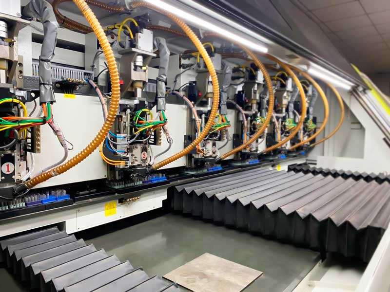
ESD Audit for PCB Assembly: What to Measure and Where An esd audit is a measurement exercise, and it fails when it turns into a paperwork exercise. The written program, the signs and the training records are necessary, but they do not protect a board. What protects the board is…
Continue Reading

Electrical Test Fixture Design: Probe Pitch and Grid Density

  • By Frank guo
  • 2026年 9月 14日
  • PCB Assembly
  • No Comments
Electrical Test Fixture Design: Probe Pitch and Grid Density An electrical test fixture holds a bare board and presses a bed of probes onto its test points so that every net can be checked for continuity and isolation in a single pass. The fixture is where the electrical test either…
Continue Reading

PCB Etch Factor Plan: Laying It Out First

  • By 杰夫
  • 2026年 9月 14日
  • PCB Assembly
  • No Comments
PCB Etch Factor Plan: Laying It Out First Buyers and engineers often focus on the finished product and forget the production line behind it. In practice, most field failures can be traced back to process decisions made during assembly. Understanding PCB etch factor plan gives you a practical advantage when…
Continue Reading
PCB Surface Finish

Oxygen Concentration: Design Rules and Process Limits

  • By Frank guo
  • 2026年 9月 14日
  • PCB Assembly
  • No Comments
Oxygen Concentration: Design Rules and Process Limits The oxygen concentration inside a reflow oven decides how much of the flux is consumed by the atmosphere rather than by the solder. At the 210,000 ppm of ordinary air, oxidation competes with wetting throughout the profile; at 1,000 ppm in a nitrogen…
Continue Reading

Anodic Bleed Under Conformal Coating: Causes and Controls

  • By Frank guo
  • 2026年 9月 14日
  • PCB Assembly
  • No Comments
Anodic Bleed Under Conformal Coating: Causes and Controls Anodic bleed is the dark, sometimes glassy track that appears along a conductor on a coated assembly after the board has spent time under bias in humid air. It is a corrosion product rather than a coating defect, and it belongs to…
Continue Reading
PCB Grounding

Solder Resist Dam Design: Dam Width and Component Spacing

  • By Frank guo
  • 2026年 9月 14日
  • PCB Assembly
  • No Comments
Solder Resist Dam Design: Dam Width and Component Spacing A solder resist dam is the strip of mask that separates two adjacent openings on a board. It prevents solder from bridging between pads during assembly, keeps the paste on the pad during printing, and provides the electrical isolation the design…
Continue Reading

Copper Contamination in the Solder Pot: Signs and Limits

  • By Frank guo
  • 2026年 9月 14日
  • PCB Assembly
  • No Comments
Copper Contamination in the Solder Pot: Signs and Limits Copper contamination is the slowest and most predictable way for a wave soldering bath to drift out of specification. Copper dissolves into the molten alloy from every plated through-hole, every exposed pad and every tinned lead that passes over the wave,…
Continue Reading

Panel Utilization and Routing Margin in PCB Fabrication

  • By Frank guo
  • 2026年 9月 14日
  • PCB Assembly
  • No Comments
Panel Utilization and Routing Margin in PCB Fabrication Panel utilization is the share of the panel area that ends up as delivered boards, and it is set at the moment the board outlines are nested. Everything else on the panel, the process edge, the gaps between boards, the tabs, the…
Continue Reading

Surface Finish Shelf Life: Storage and Solderability Control

  • By Frank guo
  • 2026年 9月 14日
  • PCB Assembly
  • No Comments
Surface Finish Shelf Life: Storage and Solderability Control Every board finish changes from the day it is applied. Oxide grows on the surface, intermetallic compounds grow between the finish and the copper beneath it, and the result is a surface that solders less readily than it did on the day…
Continue Reading
through-hole PCB assembly

Reflow Conveyor Vibration: Where Components Move

  • By Frank guo
  • 2026年 9月 14日
  • PCB Assembly
  • No Comments
Reflow Conveyor Vibration: Where Components Move Conveyor vibration is one of the few reflow variables that leaves no trace in the profile. The thermocouple records the peak temperature, the zones hold their setpoints and the boards come out at the right rate, yet a handful of small parts have moved…
Continue Reading
1 … 402 403 404 … 1,626

Search Posts

Categories

  • Electronic Materials
  • Electronical Engineering
  • Industrial Control
  • PCB Assembly
  • PCB Design
  • PCB Manufacturing

Recent Posts

Cheap PCB Costs: PCB Design, PCB Manufacturing & SMT vs TH Guide

Cheap PCB Costs: PCB Design, PCB Manufacturing & SMT vs TH Guide

Jelly - 2026年 9月 30日
Cheap PCB Costs: PCB Design, PCB Manufacturing & SMT vs TH Guide

Cheap PCB Costs: PCB Design, PCB Manufacturing & SMT vs TH Guide

Jelly - 2026年 9月 30日
NPI Manufacturing Delays: PCB Design, PCB Manufacturing & EMS Guide

NPI Manufacturing Delays: PCB Design, PCB Manufacturing & EMS Guide

Jelly - 2026年 9月 30日

Tags

AOI inspection automotive electronics automotive PCBA quality automotive standards box build assembly component mounting component procurement component supplier conformal coating defect prevention DFM checks DFM review e-bom management electronic component shortage electronic manufacturing services electronic manufacturing standards Electronic Materials electronics design best practice electronics manufacturing capacity electronics sourcing high volume production industrial electronics insertion mount manufacturability review mass production quality mixed technology PCB PCBA inspection PCBA prototype PCBA turnkey PCBA volume pricing PCB Design PCB layout rules PCB Manufacturing PCB sourcing power electronics PCB printed circuit board prototype quick turn PCB reflow soldering SMT assembly quality SMT production solder paste inspection solder paste printing surface mount technology vehicle electronics wave soldering
GOPCBA-logo

As a professional China PCB assembly manufacturer, we provide a full range of electronic manufacturing services from PCB fabrication, PCBA to OEM/ODM, including PCB design, PCB layout, rapid PCBA prototyping, components procurement, SMT/ THT assembly, china pcb assembly, china pcb prototype, PCBA testing and box build assembly.

Linkedin Facebook-f X-twitter Youtube Instagram

PCB ASSEMBLY

  • Prototype PCB Assembly
  • Low Volume PCB Assembly
  • High Volume PCB Assembly
  • Turnkey PCB Assembly
  • SMT PCB Assembly
  • Through-Hole PCB Assembly
  • Mixed Technology PCB Assembly
  • Flex PCB Assembly

OUR SERVICES

  • PCB Design/Layout
  • PCB Manufacturing
  • Rapid PCBA Prototyping
  • Components Procurement
  • Conformal Coating
  • PCBA Testing
  • Box Build Assembly
  • Wire & Cable Harness Assembly

TECHNICAL SUPPORT

  • About Us
  • Quality Management
  • Artificial Intelligence PCBA
  • Industrial PCBA
  • IOT PCBA
  • Medical PCBA
  • Energy PCBA
  • Telecommunications PCBA

Copyright © 2026. Shenzhen Kingda Electronics Co., LTD  All rights reserved. 

  • Sitemap
  • Terms of Service
  • Privacy Policy
Zmdi Zmdi-email Phone-square Whatsapp Weixin
x

ABOUT US

Progressively maintain extensive infomediaries via extensible nich. Capitalize on low hanging fruit. a ballpark value added is activity to beta test. Override the digital divide with additional click throughs from fruit.

LOCATIONS

map

New York Office

+07 554 332 322
contact@example.com
office@example.com
37 San Fairport, NY 14450, New York City
All Locations

FOLLOW US