
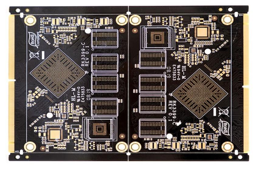
SMT Stencil Tension: How Tight the Mesh Is Modern electronics depend on boards that are assembled correctly the first time. Every product – a phone, a charger, a medical instrument or an industrial controller – relies on thousands of solder joints that must conduct current for years. This article explains…
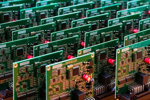
Solder Beading and Solder Ball Defects Two Different Defects Solder balls and solder beading are usually lumped together and should not be. A solder ball is a small sphere of alloy sitting on the surface, often on or beside a solder mask feature, and it is a contamination and short-circuit…
PCB Copper Trace Differential Impedance: The Pair Value Electronics manufacturing has become a discipline of small details. Solder paste volumes, placement accuracy, temperature profiles and inspection limits all add up to the final result. This guide looks at PCB copper trace differential impedance from the perspective of a PCBA factory…
Conductive Anodic Filament: CAF Failure Explained What CAF Is Conductive anodic filament is a copper-containing path that grows inside the laminate along the resin and glass interface, from an anode toward a cathode, while the board is under bias in a humid environment. It is not a surface phenomenon and…
Selective Soldering: Process and Design Rules Why Selective Soldering Exists Modern boards are mostly surface mount, but they almost always carry a few through-hole parts: connectors that must survive insertion force, transformers, relays, power terminals and parts that are simply cheaper in a leaded package. Those joints still have to…
SMT Reflow Solder Joint Grain Size: The Crystals in the Solder Buyers and engineers often focus on the finished product and forget the production line behind it. In practice, most field failures can be traced back to process decisions made during assembly. Understanding SMT reflow solder joint grain size gives…
Reflow Profile Design for Mixed Assemblies What the Profile Actually Controls A reflow profile is the temperature the assembly experiences against time, and it does three jobs at once. It has to bring every joint to a temperature above the melting point of the alloy for long enough that the…
PCB Surface Finish Thickness Control: Holding the Finish Depth Electronics manufacturing has become a discipline of small details. Solder paste volumes, placement accuracy, temperature profiles and inspection limits all add up to the final result. This guide looks at PCB surface finish thickness control from the perspective of a PCBA…
SMT Placement Offset Correction: Moving the Part Back on Center Electronics manufacturing has become a discipline of small details. Solder paste volumes, placement accuracy, temperature profiles and inspection limits all add up to the final result. This guide looks at SMT placement offset correction from the perspective of a PCBA…
PCB Via Pad Size Calculation: Sizing the Pad for the Hole Buyers and engineers often focus on the finished product and forget the production line behind it. In practice, most field failures can be traced back to process decisions made during assembly. Understanding PCB via pad size calculation gives you…