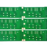
Design for Test on PCBA Assemblies
Testability is a design property, and it is one of the few that cannot be added after the fact. Once the board is laid out, the nets that can be reached are fixed, and no amount of test engineering will recover access that the layout did not provide. Designing for test is about deciding, in advance, what has to be measurable.
Why Access Matters
An assembly can be tested in two ways. Functional test exercises the product as it will be used, checking that the outputs respond correctly to the inputs. In-circuit test measures individual components and nets directly, using physical access to the board.
Functional test tells you the product does not work. In-circuit test tells you why. Without access, a fault is a symptom that has to be traced by hand, and the diagnosis time is what makes an untestable board expensive. Our <a href="https://www.gopcba.com/pcb-electrical-test-coverage/” title=”PCB electrical test coverage”>PCB electrical test coverage article describes what each method can reach.
Test Points and Their Requirements
A test point is a pad, usually a small one without a component on it, that a probe can contact. Its size and spacing are set by the fixture probe, not by the electrical requirement, so the layout must use the dimensions the test house specifies rather than the smallest pad available.
Test points also need clearance around them. A probe needs a straight approach, so a test point placed under a tall component or between two connectors cannot be reached even though it exists on the board. Our layout tips article describes the spacing discipline that makes placement reliable.
<img src="https://www.gopcba.com/wp-content/uploads/2026/09/61.jpg" alt="test points and a bed of nails fixture for PCBA testing” />
Bed of Nails Fixtures
A bed of nails fixture holds spring loaded probes on a grid that matches the test points. It contacts every point at once, which makes the test fast, and it requires a fixture to be built for each board design.
The fixture is a real cost, and it is justified where the production volume is high. For a small batch, the fixture cost per board is prohibitive, which is why low volume production uses flying probe test where the probes move to each point in turn. The trade is speed against tooling cost.

One Side or Two
Test points on a single side allow a simpler fixture with a single probe plate, which is cheaper to build and easier to maintain. Test points on both sides require a double sided fixture, which is more expensive and slower to load.
Single sided access is therefore worth designing for, even at the cost of a little routing effort. Where a net is only reachable on the underside, the question is whether the net genuinely needs to be probed, or whether functional test covers it adequately. Our routing techniques article describes how that decision is made during layout.
Deciding Coverage
Not every net needs a test point. Power nets, ground and nets that are already covered by functional test can be omitted, and the effort is better spent on nets whose failure would be hard to detect otherwise.
The useful criterion is consequence. A net that would cause a functional failure and cannot be observed another way deserves access. A net that is verified by the functional test anyway does not. Deciding this early keeps the test point count manageable and the fixture affordable.
Programming and Boundary Scan
Where a design includes programmable devices, boundary scan can test connections without physical access to every net. It uses the device’s own scan chain to drive and observe pins, which reduces the number of test points required.
Boundary scan is not a complete replacement for access, because it requires the devices in the chain to be functional and the chain to be intact. Combined with a smaller set of test points, however, it can cover a board that would otherwise need a very dense fixture.
Test Point Rules to Apply During Layout
Applying a consistent set of rules during the layout is what keeps a board testable without a later revision. The following cover the majority of the practical requirements:
- Place test points on a 2.54 millimetre grid where possible, so the fixture can be built conventionally.
- Keep test points at least the probe clearance away from tall components and from board edges.
- Group test points in an accessible area rather than scattering them across the assembly.
- Add test points to the schematic as symbols, so the netlist and the layout stay consistent.
- Verify that each test point is on the correct net after any late layout change.
- Keep the test point on high speed nets short, and treat it as a stub when calculating signal quality.
- Confirm that the test point is not covered by the solder mask or by a silkscreen legend.
- Include power and ground test points for the fixture to reference.
- Record the intended test method for each net so that coverage can be reviewed.
- Confirm the fixture approach direction against the component heights on both sides.
These checks cost minutes during the layout and remove the risk of building a fixture for a board that cannot be probed. Our design release checklist covers the review that confirms them.
Bringing Design for Test Into the Layout
Design for test is easiest to apply when it is treated as part of the layout rather than as a review at the end. Adding test points to the schematic as symbols at the start means they appear in the netlist, they are placed during the layout and they are checked by the same design rule checking that covers everything else.
Where they are added afterwards, the process becomes a manual exercise of finding free space on an accessible layer, which is slower and less reliable. The test point count also tends to drift, because each addition is considered in isolation rather than against a plan. Our design release checklist describes the review that confirms the plan was met.
Where the assembly will be tested at more than one stage, the test points serve production and field diagnosis as well as first pass testing. A board that can be probed in service is easier to repair, and the access costs nothing beyond the area the pads occupy. Our reliability notes describe how that access supports long term support of the product.
A board that can be probed during production and again during fault diagnosis repays the small area the test points occupy more than once.
FAQ
Can test points be added after the layout is finished? Sometimes, if there is free space on an accessible layer. Where the routing is dense, adding access afterwards means a revision.
How large should a test point be? Large enough for the fixture probe the test house uses. The dimension comes from the probe specification, not from the electrical design.
Is in-circuit test always better than functional test? It is better at locating faults and worse at verifying that the product works. Most production uses both.
Do test points affect signal integrity? A test point adds a small capacitance and a stub. On high speed nets it should be kept short or replaced by a via shared with another purpose.
Who should decide the test strategy? The designer, in consultation with the test engineer, and the decision should be made before the layout rather than after it.