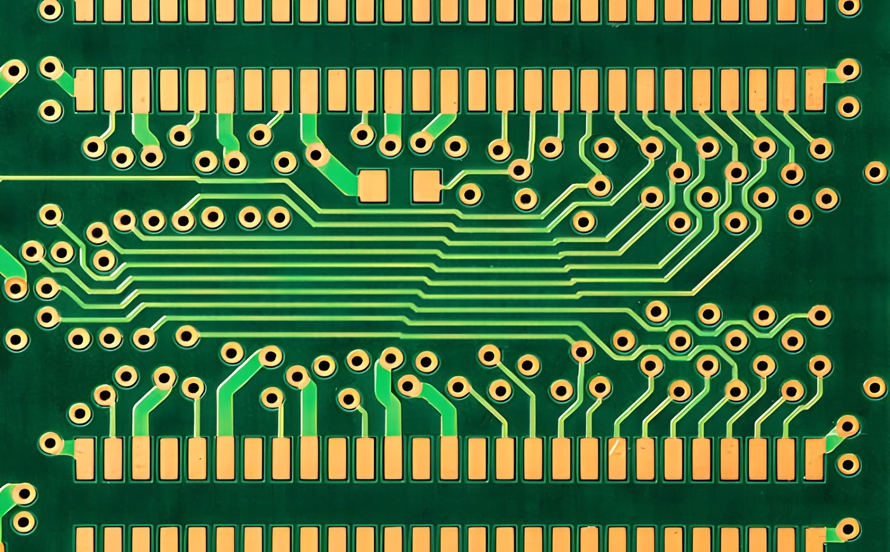
ENIG Surface Finish: PCB Design, PCB Manufacturing & ENIG Plating
Modern PCB Manufacturing processes continuously adopt new technologies and process improvements to meet increasingly complex design requirements and achieve consistent product performance. Every stage of PCB fabrication and assembly is carefully controlled because each process can influence the electrical, mechanical, and long-term reliability of the finished board.
PCB materials and exposed copper surfaces are sensitive to environmental conditions such as oxygen, moisture, contaminants, and chemicals. Without appropriate protection, exposed copper can oxidize and deteriorate, affecting solderability and long-term reliability.
PCB surface finishes provide an important protective layer over exposed copper pads. They help prevent oxidation, maintain solderability during storage and assembly, protect the copper surface, and provide an appropriate interface for soldering and, in some applications, wire bonding or contact applications.
Among commonly used surface finishes—including HASL, OSP, immersion tin, immersion silver, ENIG, and ENEPIG—ENIG surface finish has become a widely adopted option for fine-pitch, BGA, HDI, and other applications where a flat and stable solderable surface is required.
What Is ENIG Surface Finish?
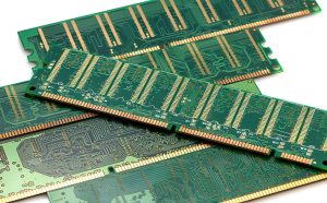
ENIG (Electroless Nickel Immersion Gold) is a two-layer metallic surface finish applied to exposed copper areas on a PCB.
It consists primarily of:
- An electroless nickel layer
- A thin immersion gold layer
The nickel layer acts as a barrier between the copper and solder while providing a durable surface for soldering. The immersion gold layer protects the nickel from oxidation during storage and handling.
Unlike electroplated gold, the immersion gold layer is intentionally very thin. During soldering, most of the gold dissolves into the solder, leaving the nickel layer as the primary barrier between the copper and solder.
Typical ENIG thicknesses depend on the applicable specification and application. A commonly encountered manufacturing range is approximately 3–6 µm for nickel and around 0.05–0.15 µm for immersion gold, although customer specifications and applicable IPC requirements may define different targets and acceptance limits.
The combination of a nickel barrier layer and a thin gold protective layer gives ENIG several important characteristics:
- Excellent surface flatness
- Good solderability
- Good oxidation resistance
- Long shelf life when properly stored
- Compatibility with fine-pitch components
- Suitable surface for BGA and HDI applications
- Good dimensional consistency
For these reasons, ENIG is frequently selected during PCB Design when fine-pitch assembly and surface-planarity requirements are important.
How Does the ENIG Process Work?
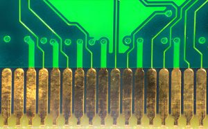
ENIG is produced through a sequence of chemical surface-treatment steps.
1. Copper Surface Preparation
The exposed copper must first be cleaned to remove oxides, organic contaminants, and other residues.
Proper surface preparation is essential because contamination can interfere with subsequent nickel deposition.
2. Electroless Nickel Deposition
A chemical nickel plating process deposits a controlled nickel-phosphorus alloy layer onto the exposed copper.
The nickel layer serves several purposes:
- Prevents direct copper-solder interaction
- Provides a stable solderable surface
- Protects the underlying copper
- Improves surface durability
- Provides a foundation for the immersion gold layer
Bath chemistry, temperature, pH, phosphorus content, plating time, and other parameters must be carefully controlled.
3. Immersion Gold Deposition
After nickel deposition, the board enters an immersion-gold bath.
Gold is deposited through a displacement reaction between the nickel surface and gold ions. Because the process is self-limiting, the resulting gold layer is very thin.
The gold protects the nickel from oxidation during storage and handling and provides a clean surface for assembly.
4. Inspection and Quality Control
After plating, manufacturers should inspect the surface for:
- Uneven plating
- Discoloration
- Pitting
- Surface contamination
- Poor deposition
- Nickel corrosion
- Gold thickness variation
For high-reliability products, additional cross-sectional analysis and plating-thickness verification may be used.
Long-Term Reliability of ENIG Solder Joints
One of the main reasons ENIG is widely used is its combination of surface flatness, solderability, and environmental stability.
When properly manufactured, ENIG can provide a reliable soldering interface for applications exposed to thermal cycling and environmental changes.
Potential application areas include:
- Automotive electronics
- Industrial control systems
- Telecommunications
- Aerospace electronics
- Defense electronics
- Medical electronics
- Consumer electronics
- High-density computing equipment
During soldering, the thin gold layer dissolves into the solder, while the nickel layer acts as the underlying barrier. The resulting solder interface must be evaluated according to the specific solder alloy, assembly process, thermal profile, and applicable reliability requirements.
ENIG should therefore not be considered a guarantee of long-term reliability by itself. PCB material selection, pad geometry, solder paste, reflow profile, component package, PCB assembly quality, and environmental conditions all contribute to solder-joint reliability.
ENIG vs. Other PCB Surface Finishes
Choosing the correct surface finish is an important part of PCB Manufacturing. Different finishes offer different combinations of cost, flatness, solderability, shelf life, and application compatibility.
ENIG vs. HASL
HASL (Hot Air Solder Leveling) is generally less expensive than ENIG and is widely used for general-purpose PCBs.
However, HASL can produce a less planar surface because molten solder is leveled across the copper features. This can make it less suitable for some fine-pitch, BGA, and very small-pad applications.
ENIG provides a much flatter surface and more consistent pad geometry.
ENIG vs. OSP
OSP (Organic Solderability Preservative) is an organic coating applied directly to exposed copper.
OSP offers:
- Low cost
- Good surface flatness
- Lead-free compatibility
- Simple processing
However, OSP is more sensitive to handling and storage conditions than metallic finishes. Multiple thermal cycles can also affect the protective coating.
ENIG generally offers better durability during handling and storage, making it attractive for products with demanding assembly or shelf-life requirements.
ENIG vs. ENEPIG
ENEPIG (Electroless Nickel Electroless Palladium Immersion Gold) adds a palladium layer between nickel and gold.
The additional palladium layer can improve certain wire-bonding and solder-joint applications and can help mitigate some nickel corrosion mechanisms associated with poorly controlled ENIG processes.
However, ENEPIG generally involves additional process steps and higher cost.
The choice between ENIG and ENEPIG should therefore be based on the specific assembly, wire-bonding, reliability, and cost requirements rather than assuming that one finish is universally superior.
ENIG vs. Immersion Silver
Immersion silver provides a relatively flat surface with good solderability and is suitable for many fine-pitch applications.
However, silver surfaces can be sensitive to sulfur-containing environments and improper storage or handling.
ENIG provides a different protection mechanism through its nickel barrier and gold layer and may be preferred where storage stability and surface durability are important.
ENIG vs. Immersion Tin
Immersion tin offers a flat surface and good solderability. However, tin surfaces require careful control of oxidation, contamination, and storage conditions.
ENIG provides a nickel barrier and gold protective layer, which can offer advantages in applications requiring a robust surface finish and extended storage capability.
Common ENIG Problems
Although ENIG is a mature and widely used surface finish, process control is extremely important. Poor chemical control or inappropriate processing can lead to surface defects and solder-joint reliability problems.
Black Pad and Nickel Corrosion
One of the most well-known ENIG-related defects is commonly referred to as Black Pad.
Black Pad is associated with excessive or localized nickel corrosion during the immersion-gold deposition process. The defect can produce a dark or abnormal nickel surface and may contribute to poor solderability or weak solder joints.
Potential contributing factors include:
- Excessive nickel corrosion
- Improper immersion-gold bath chemistry
- Poor bath control
- Excessive plating activity
- Inappropriate process parameters
- Surface contamination
Black Pad is not simply caused by a high phosphorus content in every case. It is a process-related phenomenon involving the interaction between the nickel surface and immersion-gold chemistry.
Effective control of the nickel and gold plating baths is therefore essential.
Pitting and Uneven Deposition
Surface contamination or inadequate pretreatment can result in:
- Pits
- Voids
- Uneven nickel deposition
- Uneven gold deposition
- Discoloration
- Localized corrosion
These defects can interfere with solder wetting and reduce assembly yield.
Proper cleaning, bath filtration, chemical control, and process monitoring can help reduce these risks.
Gold Embrittlement
Gold embrittlement can occur when excessive gold remains in the solder joint and contributes to the formation of brittle Au-Sn intermetallic phases.
However, the risk depends on the gold thickness, solder alloy, solder-joint volume, and assembly conditions. Therefore, a universal value such as “above 0.2 µm always causes embrittlement” should not be treated as a general rule.
Maintaining the immersion-gold thickness within the applicable specification is an important part of ENIG process control.
Storage and Shelf-Life Problems
ENIG generally offers good storage stability compared with some organic or less-protected finishes. However, improper storage can still degrade solderability.
Potential risks include:
- High humidity
- Sulfur contamination
- Dust
- Fingerprints
- Chemical contamination
- Damaged packaging
- Excessive exposure to air and moisture
The manufacturer’s specified storage conditions should therefore be followed.
ENIG Storage and Handling Best Practices
Proper handling is essential for preserving the solderability of ENIG-finished PCBs.
Recommended practices include:
Control Temperature and Humidity
Store PCBs in a clean, dry environment within the storage conditions specified by the manufacturer or applicable product requirements.
Use Appropriate Packaging
Moisture-barrier and protective packaging can help prevent contamination and environmental exposure during transportation and storage.
For sensitive products, packaging may include:
- Moisture-barrier bags
- Desiccants
- Humidity indicators
- ESD-safe packaging where required
- Clean protective separators
Minimize Direct Handling
Avoid touching finished ENIG surfaces with bare hands. Fingerprints and skin oils can contaminate the surface and potentially affect solderability.
Follow the Manufacturer’s Shelf-Life Guidance
Storage life depends on the surface finish specification, packaging method, environmental conditions, and manufacturer requirements. Instead of applying a universal shelf-life period, follow the specific storage and assembly recommendations supplied with the PCB.
How to Improve ENIG Solderability
To obtain consistent soldering performance from ENIG-finished PCBs, both PCB fabrication and PCB assembly processes must be controlled.
Select a Qualified PCB Manufacturer
Choose a manufacturer with controlled chemical processes, calibrated inspection equipment, and documented process controls.
The manufacturer should be capable of monitoring:
- Nickel thickness
- Gold thickness
- Bath chemistry
- Plating uniformity
- Surface cleanliness
- Corrosion
- Solderability
Verify Surface Quality
Before PCB Assembly, inspect the finished PCB for:
- Uneven gold
- Dark areas
- Pitting
- Scratches
- Contamination
- Abnormal discoloration
- Surface defects
Control Nickel and Gold Thickness
The nickel layer must provide adequate protection and barrier performance, while the gold layer must remain within the applicable specification.
Excessive gold thickness can increase material cost and may affect solder-joint metallurgy, while insufficient gold may reduce protection of the nickel surface.
Optimize the Reflow Profile
The reflow temperature profile should be compatible with:
- PCB materials
- ENIG surface finish
- Solder alloy
- Component package
- Solder paste
- Assembly equipment
Avoid unnecessary overheating or excessive time above liquidus because inappropriate thermal profiles can affect solder-joint reliability.
Control Post-Assembly Storage
After assembly, maintain appropriate environmental conditions and protect finished assemblies from excessive humidity, contaminants, and chemical exposure.
ENIG Applications
ENIG is used across a wide range of electronic products.
Automotive Electronics
ENIG can be used for automotive control modules, sensors, communication systems, and other assemblies requiring a flat and stable soldering surface.
Industrial Electronics
Industrial control boards often benefit from the combination of surface flatness, solderability, and storage stability provided by ENIG.
Aerospace and Defense Electronics
High-density and fine-pitch assemblies can use ENIG where controlled surface geometry and reliable soldering are important.
Medical Electronics
Medical electronics can use ENIG for compact, high-density circuit assemblies where consistent manufacturing and assembly quality are required.
High-Density Digital Electronics
BGA, QFN, fine-pitch components, HDI structures, and other dense layouts can benefit from the planar surface provided by ENIG.
Advantages and Limitations of ENIG
| Feature | ENIG Characteristics |
|---|---|
| Surface flatness | Excellent |
| Fine-pitch compatibility | Excellent |
| BGA compatibility | Excellent |
| Oxidation protection | Good |
| Solderability | Good to excellent when properly processed |
| Storage stability | Generally good |
| Process complexity | Higher than HASL and OSP |
| Cost | Generally higher than HASL and OSP |
| Main process risk | Nickel corrosion / Black Pad if poorly controlled |
| Typical applications | HDI, BGA, fine-pitch, industrial, automotive, aerospace, medical |
Conclusion
ENIG surface finish has become one of the most widely used metallic surface finishes in modern PCB Manufacturing because it combines excellent surface flatness, good solderability, oxidation protection, and compatibility with fine-pitch components.
The combination of an electroless nickel barrier and a thin immersion-gold layer makes ENIG particularly useful for BGA, HDI, fine-pitch, and other high-density PCB applications.
However, ENIG performance depends heavily on process control. Nickel corrosion, Black Pad, uneven deposition, contamination, excessive gold, and improper storage can all affect solderability and long-term reliability.
For engineers, ENIG should therefore be considered during the PCB Design stage together with pad geometry, component package requirements, assembly process, storage conditions, and reliability targets. For manufacturers, strict control of cleaning, nickel deposition, immersion-gold chemistry, thickness, inspection, and documentation is essential.
With controlled fabrication and assembly processes, ENIG can provide a stable and reliable surface finish for demanding electronic products.Kingda supports PCB fabrication and assembly projects requiring fine-pitch processing, controlled surface finishes, high-density layouts, and reliable manufacturing quality.