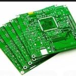
Fine Line PCB Trace Cost Guide: 3mil, 4mil and 5mil Prices
A fine line PCB trace cost is usually higher than the cost of a conventional trace because the manufacturing process requires better imaging, tighter etching control, more accurate registration, and lower defect tolerance. Products such as smartphones, automotive electronics, medical devices, 5G communications, AI hardware, and high-performance computing systems continue to demand 5 mil, 4 mil, and 3 mil traces so more functions fit into a smaller board. Understanding how trace width changes price helps engineers choose a practical design target instead of automatically selecting the narrowest line.
This 2026 guide compares 3 mil, 4 mil, and 5 mil trace pricing, explains the main cost drivers, and recommends ways to reduce fine-line PCB manufacturing expense while maintaining quality.
What Is a Fine Line PCB Trace?
A PCB trace is the copper conductor that connects ICs, resistors, capacitors, power networks, and signal paths. Standard boards commonly use 6 mil to 10 mil traces. Fine-line boards use widths from roughly 5 mil down to 3 mil, while ultra-fine-line technology moves below 3 mil for semiconductor packaging and advanced computing.
Trace width affects current-carrying ability, signal integrity, thermal behavior, routing density, and manufacturability. Narrower traces allow more routing in a small area, but they require a fabrication line with higher precision and stricter process limits.
Fine-line capability is normally found in HDI, high-density consumer, automotive, medical, and communications boards. The technology is also linked with small vias, tight component pitch, and controlled impedance.
Why Narrow Traces Cost More
Using less copper does not automatically reduce the PCB price. The added cost comes from manufacturing precision. A 3 mil trace leaves very little room for variation. Slight over-etching can make the conductor too thin and create an open risk, while under-etching can leave copper residue and cause shorts.
Fine lines usually require laser direct imaging or high-accuracy exposure, stable chemistry, frequent process checks, and tighter layer registration. All of these steps add equipment and engineering cost.
Yield is another important factor. Conventional boards have mature processes and low scrap rates. When trace widths become very small, more boards may fail inspection, so the manufacturer must either raise prices or accept a higher scrap cost.
2026 Trace Width Price Comparison
5 mil traces are the entry level of fine-line technology. They are suitable for many industrial, automotive, communications, and consumer designs. Typical prototype pricing may range from USD 80 to USD 250 per panel, with small-volume production around USD 3 to USD 15 per board and medium-volume production around USD 1 to USD 6 per board.
4 mil traces require better process capability. Prototype prices commonly fall between USD 120 and USD 350 per panel, small-volume production between USD 5 and USD 25 per board, and medium production between USD 2 and USD 10 per board. Compared with 5 mil designs, 4 mil traces often add about 15% to 35% in cost.
3 mil traces are reserved for HDI, AI hardware, high-end mobile devices, and aerospace applications. Prototype costs may range from USD 200 to USD 600 per panel, with small-volume production from USD 10 to USD 50 per board. Compared with standard 6 mil traces, 3 mil lines can increase cost by 40% to 100% or more.
These ranges depend on size, layer count, material, quantity, finish, and via structure, so they should be used only for early budgeting and confirmed with actual Gerber-based quotations.
Factors That Drive Fine-Line Cost
Layer count has a direct effect. A two-layer board with fine lines is simpler than an eight-layer board because every inner layer must be aligned and imaged consistently. A 12-layer HDI stackup with microvias and fine lines raises cost sharply.
Copper weight also matters. Narrow traces are easier to control on 1 oz copper than on 2 oz or 3 oz copper because etching removes more metal and the process window becomes smaller. A 3 mil trace on 2 oz copper is much harder to build than a 5 mil trace on 1 oz copper.
Material choice affects cost. FR-4 is economical for many fine-line applications, while high-Tg FR-4, high-frequency laminates, and HDI build-up materials increase the quote. Surface finish is another factor because fine-pitch components need a flat, reliable finish such as ENIG or ENEPIG rather than standard HASL.
Designers should also check the routing pitch around fine-pitch components. A narrow trace between BGA pads may create little room for solder mask registration and inspection. Choosing 5 mil lines where possible, and reserving 3 mil or 4 mil for areas where BGA escape routing truly requires them, often gives the best balance between electrical performance and manufacturable cost.
Applications That Need Fine Lines
HDI boards depend on fine lines and microvias to route smartphones, tablets, and wearables. Automotive electronics use fine lines in ADAS, ECU modules, battery management, and smart cockpit systems where space and speed are important. Medical equipment needs stable, compact boards for monitors and diagnostic instruments.
High-speed communications equipment uses fine lines for low-loss signal paths with controlled impedance. AI and high-performance computing products push toward ultra-fine-line capability because advanced chips have thousands of connections and limited package area.
Fine Lines and Signal Integrity
Trace width, spacing, and reference plane affect characteristic impedance. A fine-line design must match the intended width to the stackup and copper thickness so the impedance target can be met. During fabrication, width variation changes impedance and can degrade high-speed signals.
Designers should also consider copper surface roughness, because rough copper increases loss at high frequency. Fine-line boards for RF and high-speed applications may require low-profile copper foil or controlled surface treatment.
An early PCB design and layout review can confirm that the required trace width is practical for the material, copper weight, and manufacturing process.
Signal traces and power traces should therefore be designed with separate rules. Data lines can use the finest width needed for routing and impedance, while supply and return paths should be wide enough to keep resistance and temperature rise within acceptable values.
Current Capacity and Thermal Limits
Narrow traces carry less current and generate more heat for a given current level. If the design needs higher current, the trace should be widened or the copper weight increased. Thermal design should also include nearby planes, vias, and component placement.
The combination of very narrow traces and thick copper is difficult because etching cannot easily produce fine sidewall geometry. Engineers should choose copper weight based on real current and thermal requirements rather than assuming that thin lines can be used everywhere.
How to Reduce Fine-Line PCB Cost
Avoid specifying the smallest available width unless the design truly needs it. If 5 mil routing satisfies electrical, spacing, and layout requirements, it is usually more economical and more reliable than 3 mil routing. Wider traces also leave more tolerance for normal process variation.
Optimize the stackup so signal, power, and ground layers are planned together. Reducing unnecessary layer count and via complexity lowers cost. Review pad size, via size, and component placement to avoid routing bottlenecks that force narrow lines into critical paths.
Choose a finish based on component pitch and reliability. ENIG or ENEPIG may be necessary for fine-pitch BGAs, but an OSP or immersion finish can be acceptable for simpler designs. Matching the finish to the actual assembly process prevents unnecessary expense.
Volume also influences the fine-line cost calculation. Prototype orders carry fixed engineering, tooling, and inspection costs, while production orders spread those costs across many boards. Once a 5 mil or 4 mil design is qualified, a stable high-volume PCB assembly flow helps keep the per-unit cost predictable.
Manufacturing and Quality Considerations
Fine-line production should be controlled through the whole process, not only at final AOI. Material storage, imaging, etching rate, copper grain structure, and lamination registration all affect the final trace width. Microsection and impedance checks help confirm that internal lines match the design.
Work with a factory that can review your fine-line design before tooling. The manufacturer can advise whether the line width, spacing, copper weight, and material combination are compatible with stable volume production.
During design, complete DFM review with PCB manufacturing specialists reduces the number of engineering queries and prototype iterations. A capable PCB manufacturing capability assessment shows what trace and via combinations the factory can run reliably.
Testing should cover both electrical and dimensional requirements. Continuity testing finds opens and shorts, while AOI checks visible trace defects. For fine-pitch and high-speed boards, impedance measurement and microsection verification may also be required so the manufactured lines match the electrical design.
Conclusion
Fine line PCB trace cost depends on imaging precision, etching control, layer alignment, yield, material, copper weight, and finish. 5 mil lines offer a strong balance of density and cost for many commercial products, while 4 mil and 3 mil lines add cost for high-density and high-performance applications.
Selecting the narrowest possible trace is not always the best engineering decision. With proper design review and a manufacturer qualified for fine-line production, teams can achieve the required routing density without paying for capability the product does not need.