Gateway PCB Guide: Design, Manufacturing and Cost
Every smart home, connected factory, and IoT deployment depends on a quiet but essential device: the gateway that sits between local sensors and the cloud. Inside that gateway, the circuit board determines how reliably data flows, how many radios can coexist, and how long the device runs on its power budget. For engineers developing gateway hardware and for buyers sourcing it, understanding the gateway device PCB is the fastest route to a product that connects cleanly and survives years of service. This guide explains what a gateway PCB is, its core functions, board types, design priorities, manufacturing steps, cost expectations, and how to choose a manufacturer.
What Is a Gateway Device PCB?
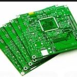
A gateway device PCB is a printed circuit board designed for equipment that bridges different networks. A typical gateway receives data from wireless sensors using protocols such as Zigbee, Z-Wave, Bluetooth, LoRa, or Wi-Fi, converts and packages that data, and forwards it over Ethernet, 4G, 5G, or fiber toward a server or cloud platform. The board must therefore carry multiple radios, a processor powerful enough to route and translate the traffic, and power circuitry able to run around the clock. Compared with an ordinary control board, a gateway PCB is optimized for data throughput, protocol handling, and signal integrity, because a dropped packet or an unstable radio link quickly becomes an invisible failure across the whole network.
Core Functions of a Gateway PCB
Several jobs define the board. Data routing and signal processing let the gateway translate between local protocols and the internet, manage addressing, and buffer bursts of sensor traffic. Power management balances always-on operation with efficiency, often using low-power sleep states when the network is idle. Connectivity support is what makes the board a gateway at all: it must integrate the specific radios the product targets, from low-power mesh radios to high-speed cellular modules. Security and reliability are increasingly part of the hardware itself, with dedicated encryption engines, tamper protection, and careful shielding that keeps each radio from interfering with the others. A gateway PCB that fails at any of these jobs undermines every device connected to it.
Types of Gateway PCBs
Gateway boards span a wide range of complexity. Simple single-layer boards appear in low-cost, low-data-rate devices with a single radio and limited processing. Multilayer boards are the norm for serious IoT gateways because high-speed Ethernet, USB, and memory buses need dedicated ground planes and controlled impedance; these designs commonly use four to eight layers. Rigid boards suit industrial and wall-mounted gateways where durability and cost matter, while flexible and rigid-flex boards are chosen for compact consumer gateways, routers with integrated antennas, and devices where the circuit must fold around the enclosure. The layer count and material grade should match the fastest signals on the board, not the marketing story.

Applications of Gateway PCBs
Gateway circuit boards appear wherever separate networks must meet. Smart home hubs use them to connect lights, locks, thermostats, and voice assistants to the home network and the cloud. Industrial automation relies on them to move real-time data between machines, PLCs, and monitoring systems on the factory floor. In 5G, cloud, and edge computing, high-performance gateway boards aggregate traffic at the edge of the network and reduce latency by processing data close to its source. Building management, agriculture, energy metering, and logistics all use gateway hardware to connect remote sensors back to central systems. In every case, the reliability of the board determines the reliability of the connection that the whole deployment depends on.
Gateway PCB Design Priorities
Gateway hardware is demanding because several high-speed and radio systems share one board. Signal integrity is the top priority: Ethernet pairs, USB, DDR memory, and radio interfaces all need controlled impedance, clean routing, and isolation from each other. Thermal management follows, because gateways often run 24 hours a day inside warm enclosures or on poles in direct sun, so copper pours, thermal vias, and airflow paths keep the processor and power stages within their limits. Power efficiency is next, especially for battery-backed or solar-powered gateways where every milliwatt matters in sleep mode. Miniaturization rounds out the list for portable and embedded IoT gateways, where board area is scarce and antennas must still perform. These priorities are exactly where a skilled PCB design and layout team earns its keep, because a gateway that loses packets or overheats in the field is expensive to fix after deployment.
Radio Coexistence and Antenna Design
Putting several radios on one board is a discipline of its own. A typical IoT gateway may carry a sub-GHz radio for sensors, a 2.4 gigahertz radio for Wi-Fi or Zigbee, and a cellular module for uplink, all operating at once. Each transmitter creates noise that can desensitize the other receivers if the layout does not manage isolation. Good designs give every antenna its own keepout area, place radios on opposite edges of the board, filter each supply rail, and use grounded shielding cans around the most sensitive modules. The antenna itself is part of the design decision: printed antennas are cheap but sensitive to enclosure and ground, ceramic chip antennas are compact, and external connectors are the most reliable for industrial products where performance is critical. RF test points on the production board let the factory verify output power and sensitivity on every unit. These details matter because a gateway that cannot hear its sensors is invisible to the user until the whole network stops reporting, which is why experienced Internet of Things PCBA teams treat radio layout as a core competency rather than an afterthought.
Manufacturing Process for Gateway PCBs
Production starts with prototyping: small batches validate the design, radio performance, and thermal behavior before volume commitment. Once approved, the boards move to volume manufacturing using surface mount assembly for the dense processor and memory circuits, with selective or wave soldering for through hole connectors and power parts. Quality control is unusually important for gateway boards because the failure modes are subtle: signal tests verify that high-speed links run without errors, radio testing checks output power and receiver sensitivity, and thermal and durability tests confirm the board survives continuous operation. Inspection should include automated optical checks and, for high-speed designs, impedance verification. A partner that runs complete PCBA testing prevents field failures that would otherwise surface as intermittent connectivity problems months after installation.
Gateway PCB Cost
The price of a gateway PCB depends on the number of radios, processor class, layer count, and production volume. A basic single-layer gateway board in small batches may cost roughly 50 to 80 dollars per batch when spread across a small prototype run. Multilayer IoT gateway boards typically land in the 120 to 250 dollar range per board for moderate volumes, depending on size and layer count, with higher prices for boards that carry many radios and a powerful processor. High-end 5G gateway boards involve precision stackups, advanced materials, and costly cellular modules, so their bare boards commonly exceed 300 dollars before assembly. The way to control cost is to match the board to the product: simplify layer count where possible, standardize the design across a product family, and consolidate orders to reach volume pricing.
Choosing a Gateway PCB Manufacturer
Because gateway boards combine RF, high-speed digital, and power circuits, choose a factory with real experience in communication products rather than a general-purpose shop. Ask about its history with IoT and telecom boards, and confirm it can handle the specific stackups and tolerances your radios need. Verify certifications such as ISO, RoHS, and IPC compliance, and check whether UL or other regional approvals apply to your product category. Prototype speed matters because gateway products often follow tight launch windows, so ask about quick-turn service. Confirm that volume pricing improves with quantity and that quotes include fabrication, assembly, and testing. A supplier that offers engineering feedback during design review and manages the whole flow, from PCB manufacturing through assembly, is easier to work with than a fragmented supply chain, because a single team can trace a radio performance problem back to the layout, the material, or the process.

Future Trends in Gateway PCBs
Gateway hardware is evolving quickly along with the networks it serves. AI-enabled gateways are beginning to run lightweight machine learning models locally, which adds accelerators and more memory to the board. 6G research is pushing radio front ends toward higher frequencies and new materials. Environmental requirements are driving halogen-free laminates, lead-free assembly, and designs that use less energy in always-on deployments. Security is moving deeper into hardware with trusted platform modules and encrypted storage. These trends raise the technical bar for gateway boards, and manufacturers that combine RF experience, high-speed digital capability, and disciplined testing will be best positioned to build them.
Mechanical and Environmental Design
Gateway hardware often lives in harsh places: factory floors, utility poles, outdoor cabinets, and wall boxes with little airflow. The board design must therefore match the mechanical and environmental plan. Power-over-Ethernet is common in commercial gateways because one cable delivers both data and power, while industrial devices often accept a wide DC input range and need surge protection on the incoming lines. Component placement should respect the enclosure height, keep heat-generating parts near the heatsink or vents, and leave space for the connectors and antenna cables. For outdoor or dusty environments, conformal coating protects the board from condensation and contamination, and wide-temperature components keep the device reliable between freezing winters and hot summers. Vibration and shock resistance matter in vehicles and machinery, where connectors and large components should be mechanically supported. Finally, the production process must be matched to these requirements, so confirm that the factory can apply coatings, run the extended temperature tests, and handle the final PCB assembly with the same quality controls used for the bare boards.
Frequently Asked Questions
Q1. How long does a gateway PCB last? A well-built gateway board typically lasts 5 to 10 years, depending on operating temperature, power quality, and workload.
Q2. How can I reduce gateway PCB manufacturing cost? Order in larger volumes, simplify the layer stackup, standardize the design across a product family, and work with a supplier that offers volume pricing with complete quotes.
Q3. Can the same PCB design serve different gateway products? Often yes with adjustments for the radio modules and protocols, because antenna layout, processor choice, and power requirements differ between Wi-Fi, Zigbee, LoRa, and 5G variants.
Q4. Why does my gateway lose connections intermittently? Intermittent loss is frequently caused by radio interference, marginal power delivery, or antenna mismatch, all of which trace back to layout decisions on the PCB.
Q5. Do gateway boards need special materials? High-speed Ethernet and memory signals need controlled-impedance laminates, and RF sections may require low-loss materials depending on frequency and sensitivity.
Conclusion
A gateway PCB is the quiet backbone of the connected world. It carries the radios, routes the data, manages the power, and protects the network, and its design quality decides whether a smart home or an industrial deployment runs flawlessly or fails invisibly. Understanding the functions, design priorities, manufacturing steps, and cost drivers helps engineers and buyers specify boards with confidence. With disciplined RF and high-speed layout, quality fabrication, and thorough testing, a gateway board will keep every device on the network talking for years.