Gerber to PCB: How to Convert Gerber Files into an Editable PCB Design
In electronic engineering and PCB manufacturing, Gerber files are one of the most widely used formats for communicating fabrication data to a PCB manufacturer. They describe the physical artwork required to manufacture a circuit board, including copper layers, solder mask, silkscreen, and other fabrication features.
Gerber files can be thought of as a standardized manufacturing language for PCBs. However, what happens when you need to work in the opposite direction and convert Gerber to PCB?
This situation is more common than it may initially seem. An engineer may lose the original CAD project, need to modify an older circuit board for which only manufacturing data remains, or need to reconstruct a legacy design for continued production.
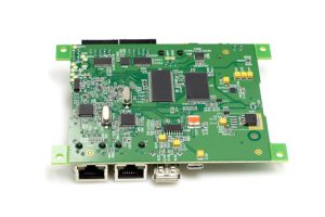
In these cases, learning how to convert Gerber files to PCB files can be extremely useful.
However, there is an important technical distinction: Gerber files cannot normally be converted back into the original PCB design with 100% fidelity. Gerber data primarily describes the final physical artwork, while a native PCB design file contains additional design information such as component relationships, net names, design rules, footprints, schematic associations, and design intent.
Therefore, a more accurate description is Gerber-to-PCB reconstruction rather than simple file conversion.
This guide explains what Gerber and PCB files contain, why reconstruction may be necessary, and how to rebuild an editable PCB design from Gerber and drill data.
What Are Gerber Files?
Gerber files are standardized manufacturing data files used to represent individual physical layers of a PCB.
A typical Gerber package may contain separate files for:
- Top copper
- Bottom copper
- Internal copper layers
- Top solder mask
- Bottom solder mask
- Top silkscreen
- Bottom silkscreen
- Board outline
- Other fabrication artwork when required
Modern PCB manufacturing commonly uses RS-274X or Gerber X2 formats.
Each file generally represents two-dimensional graphic information rather than the complete logical design of the circuit.
For example, a copper Gerber file can show where copper features should be fabricated, but it does not necessarily tell you:
- Which net a trace belongs to
- Why two components are connected
- Which component library was used
- Which schematic symbol corresponds to a footprint
- What design rule was applied
- What the original designer intended
Drill data is normally supplied separately, often in Excellon format, to define hole locations and tool sizes.
This distinction becomes extremely important when attempting Gerber to PCB conversion.
What Is a Native PCB File?
A native PCB design file is created and edited using PCB design software such as Altium Designer, KiCad, Cadence, or other EDA platforms.
Unlike Gerber data, a native PCB project can contain much more information about the design.
Depending on the software, it may include:
- Component footprints
- Component references
- Pad definitions
- Net names
- Connectivity information
- Board dimensions
- Layer stackup
- Design rules
- Routing information
- Via definitions
- Component properties
- Schematic relationships
- Manufacturing constraints
This information makes the design editable.
For example, if you want to move a connector, change a trace, replace a component footprint, or modify a copper layer, working from the native PCB design is significantly easier than modifying isolated Gerber artwork.
Why Convert Gerber to PCB?
There are several practical reasons why engineers may need to reconstruct a PCB from Gerber files.
1. The Original PCB Design Files Are Lost
A company may have an old circuit board but no longer have access to the original CAD project.
The available documentation may consist only of:
- Gerber files
- Drill files
- Fabrication drawings
- Assembly drawings
- Bill of materials
Reconstructing an editable PCB design can provide a new working design database for future modifications.
2. Legacy PCB Projects
Older electronic products can remain in production for many years.
If the original CAD software or project files are no longer available, Gerber to PCB reconstruction may provide a practical way to recreate the physical board.
3. PCB Reverse Engineering
Engineers may need to analyze an existing PCB to understand its physical structure or create a compatible replacement.
Gerber and drill data can provide useful information about:
- Layer structure
- Copper routing
- Pad locations
- Via locations
- Board dimensions
- Hole patterns
However, reverse engineering a PCB requires careful validation because the manufacturing files may not contain the complete electrical design.
4. Design Modification
A manufacturer or engineering team may need to modify an existing board but only have the manufacturing data.
Reconstructing the design into an editable PCB format makes future changes easier.
5. Design Recovery
Rebuilding a design from available manufacturing data can also serve as a form of design recovery when the original project database is unavailable.
Gerber to PCB: What Can and Cannot Be Recovered?
Before starting the reconstruction process, it is important to understand the limitations.
| Information | Usually Recoverable From Gerber Data? |
|---|---|
| Copper geometry | Yes |
| Solder mask openings | Yes |
| Silkscreen graphics | Yes |
| Board outline | Usually |
| Drill locations | Yes, from drill data |
| Hole sizes | Yes, from drill data |
| Pad shapes | Generally |
| Trace geometry | Generally |
| Component reference markings | Often |
| Net names | No |
| Original schematic | No |
| Original component libraries | No |
| Original design rules | No |
| Design intent | No |
| Exact component values | Usually no |
| Original layer stackup | Not necessarily |
| Original CAD constraints | No |
This is why Gerber to PCB conversion should be treated as a reconstruction process.
The more supporting documentation you have, the more accurately the original design can be rebuilt.
How to Convert Gerber to PCB Files
The exact workflow depends on the PCB software and the quality of the available manufacturing data. In general, the process involves importing the manufacturing layers, reconstructing the board structure, recreating connectivity, and validating the result.
Step 1: Collect All Available Manufacturing Data
Before starting the reconstruction, collect as much information as possible.
Ideally, you should have:
- All copper Gerber files
- Solder mask files
- Silkscreen files
- Board outline
- Excellon drill files
- Fabrication drawings
- Assembly drawings
- Bill of materials
- Original component placement information
- Layer stackup information
Do not begin with only one copper layer if the complete manufacturing package is available.
Missing layers can make reconstruction significantly more difficult.
Step 2: Choose Suitable PCB Design Software
Select an EDA platform capable of importing or referencing Gerber and drill data.
Potential options include:
- KiCad
- Altium Designer
- Cadence PCB tools
- Other professional PCB design systems
- Specialized Gerber/CAM tools
The important point is to distinguish between a Gerber viewer, a CAM system, and a PCB editor.
A Gerber viewer is primarily designed to inspect manufacturing artwork. It does not necessarily create a fully editable native PCB design.
Some EDA and CAM tools can import Gerber geometry, but the exact reconstruction capabilities vary.
Step 3: Import the Gerber Layers
Load all available Gerber files into the appropriate software.
Map each file to its correct function:
- Top copper
- Bottom copper
- Internal copper layers
- Top solder mask
- Bottom solder mask
- Top silkscreen
- Bottom silkscreen
- Board outline
Pay close attention to layer polarity and file orientation.
Incorrect layer mapping can make the entire reconstruction inaccurate.
Step 4: Import the Drill Data
Next, import the Excellon drill file.
The drill data helps reconstruct:
- Through-hole locations
- Via locations
- Mounting holes
- Mechanical holes
- Hole diameters
Check that the drill coordinates align correctly with the copper pads.
If the drill pattern does not match the imported copper artwork, stop and investigate the issue before continuing.
Possible causes include:
- Incorrect units
- Coordinate-format mismatch
- Incorrect origin
- Incorrect scaling
- Mirrored data
- Incorrect drill-file interpretation
Step 5: Reconstruct the Board Outline
Create or verify the board outline in the native PCB editor.
The outline should accurately represent:
- Overall board dimensions
- External shape
- Rounded corners
- Cutouts
- Slots
- Mounting holes
- Other mechanical features
Whenever possible, compare the reconstructed dimensions with the original fabrication drawing.
Step 6: Recreate Pads, Tracks, and Vias
The imported Gerber artwork provides the physical geometry needed to reconstruct copper features.
Depending on the software and workflow, you may need to convert or redraw:
- Tracks
- Pads
- Vias
- Copper pours
- Polygon areas
- Component land patterns
This can be one of the most time-consuming parts of the Gerber to PCB reconstruction process.
Simple boards can be reconstructed relatively quickly, while dense multilayer boards with fine-pitch components may require extensive manual work.
Step 7: Recreate Component Footprints
Gerber files may show pad geometry and silkscreen markings, but they generally do not contain the complete original component-library information.
Therefore, you may need to recreate or select appropriate footprints.
For each component, verify:
- Pad count
- Pad dimensions
- Pad spacing
- Component orientation
- Reference designator
- Package type
- Pin numbering
- Courtyard or mechanical clearance where applicable
Assembly drawings and the bill of materials can be extremely useful during this stage.
Step 8: Reconstruct the Net Connectivity
This is one of the most difficult parts of converting Gerber to PCB.
Gerber artwork represents physical copper but generally does not preserve the original logical netlist.
For example, two copper traces may appear connected physically, but the Gerber data does not necessarily identify the connection as a named electrical net.
You may need to reconstruct connectivity manually by analyzing:
- Copper routing
- Pads
- Vias
- Component pin assignments
- Schematic documentation
- Assembly drawings
- Datasheets
- Test points
For complex boards, this step may require substantial engineering analysis.
Step 9: Rebuild Design Rules
The original PCB design rules are normally not preserved in Gerber files.
You may therefore need to recreate appropriate rules for:
- Minimum trace width
- Minimum spacing
- Via dimensions
- Hole sizes
- Copper-to-edge clearance
- Solder mask clearance
- Differential-pair routing
- Controlled impedance
- High-voltage clearance
These rules should be based on the intended application, PCB manufacturer capabilities, applicable standards, and engineering requirements.
Do not assume that the dimensions observed in the Gerber files represent the complete original design rules.
Step 10: Reconstruct the Layer Stackup
For multilayer PCBs, determining the original stackup can be challenging.
Gerber files can identify physical copper artwork, but they may not provide complete information about:
- Dielectric thickness
- Material type
- Prepreg structure
- Core thickness
- Copper weight
- Impedance-controlled construction
If stackup information is unavailable, use fabrication documentation or consult the original manufacturer whenever possible.
For high-speed or RF designs, reconstructing the exact stackup may be especially important because dielectric thickness and material properties can directly affect impedance and signal integrity.
Step 11: Run Electrical and Design Checks
Once the PCB has been reconstructed, perform a comprehensive design review.
Check:
- Open circuits
- Short circuits
- Incorrect connections
- Trace widths
- Trace spacing
- Via locations
- Hole sizes
- Pad alignment
- Component orientation
- Board dimensions
- Layer alignment
- Solder mask openings
- Silkscreen placement
Run DRC and connectivity checks in the selected PCB design software.
If a schematic is available, compare the reconstructed PCB against it.
Step 12: Compare the Reconstructed PCB With the Original Gerber Files
This is one of the most important validation steps.
Generate new manufacturing artwork from the reconstructed PCB and compare it against the original Gerber package.
Compare:
- Copper geometry
- Pad locations
- Via locations
- Drill locations
- Board outline
- Solder mask openings
- Silkscreen
- Internal copper layers
The reconstructed PCB should closely match the original manufacturing data before it is released for production.
Challenges of Gerber to PCB Conversion
Although the process is possible, it has several limitations.
Loss of Design Intent
Gerber files describe manufacturing geometry rather than the complete engineering intent.
You may know where a trace exists without knowing why it was routed that way.
Missing Netlist
The original logical connectivity is generally not preserved.
Recreating a complete netlist can therefore require significant manual analysis.
Missing Component Information
A Gerber file does not normally tell you the exact component value, manufacturer part number, or original library footprint.
Additional documentation may be required.
Multilayer PCB Complexity
Reconstructing a multilayer PCB is considerably more difficult than reconstructing a simple two-layer board.
Internal copper routing, vias, stackup information, and impedance requirements all increase the complexity.
High-Speed PCB Challenges
For high-speed designs, simply reproducing the visible copper geometry may not be sufficient.
Signal integrity can depend on:
- Stackup
- Dielectric properties
- Trace geometry
- Reference planes
- Controlled impedance
- Via structures
- Return-current paths
Therefore, a reconstructed high-speed PCB should undergo additional engineering validation before production.
Gerber Files vs. PCB Files
Understanding the difference between these two formats helps explain why direct conversion is difficult.
| Feature | Gerber Files | Native PCB Files |
|---|---|---|
| Main purpose | PCB fabrication | PCB design and editing |
| Physical layer artwork | Yes | Yes |
| Copper geometry | Yes | Yes |
| Drill data | Usually separate | Usually integrated/referenced |
| Netlist | No | Yes |
| Component footprints | Geometry only/limited | Yes |
| Design rules | No | Yes |
| Schematic relationship | No | Often linked |
| Editable design database | No | Yes |
| Design intent | Limited | Much more complete |
| Manufacturing output | Yes | Can generate it |
In simple terms, Gerber files describe what the finished PCB should physically look like, while native PCB files contain information about how the board was designed and how it can be modified.
How to Make Gerber-to-PCB Reconstruction More Accurate
If you need to reconstruct a board from Gerber data, the following practices can improve accuracy.
Keep the Original Gerber Package Organized
Preserve all original files and do not overwrite them during reconstruction.
Create a separate working directory for the reconstructed PCB.
Gather Supporting Documentation
The more information available, the better the reconstruction.
Useful documents include:
- Schematic
- BOM
- Assembly drawing
- Pick-and-place file
- Fabrication drawing
- PCB stackup
- Component datasheets
- Previous revision documentation
Compare Against a Physical PCB
If a physical board is available, inspect it carefully.
A physical inspection can help confirm:
- Component package types
- Component orientation
- Connector locations
- Board dimensions
- Mechanical features
- Markings
However, measurements from a physical board should be treated as supporting evidence rather than automatically assumed to represent the original CAD dimensions.
Validate Before Manufacturing
Never assume that a reconstructed PCB is production-ready simply because its appearance matches the original Gerber files.
Perform DRC, connectivity checks, manufacturing review, and functional validation as appropriate.
How Kingda Can Support PCB Manufacturing
Once the reconstruction is complete, the next step is to determine whether the recovered design is suitable for production.
Kingda can support customers with PCB Manufacturing requirements by reviewing manufacturing data and helping evaluate the manufacturability of reconstructed or legacy PCB designs.
For recovered designs, important manufacturing considerations may include:
- Layer count
- Board thickness
- Copper thickness
- Trace and spacing requirements
- Minimum hole size
- Via structures
- Surface finish
- Solder mask
- Board tolerances
- Impedance requirements
- Special mechanical features
Early communication with a PCB Manufacturer can help identify potential manufacturing concerns before the reconstructed design enters production.
For legacy products, this can also provide an opportunity to review whether the original design should be reproduced as-is or updated to accommodate current component availability, manufacturing capabilities, or reliability requirements.
Frequently Asked Questions About Gerber to PCB Conversion
Can Gerber files be converted directly into a PCB file?
Some PCB design and CAM tools can import Gerber geometry, but this is generally not a complete one-click conversion into the original editable PCB project.
In most cases, additional reconstruction is required for footprints, net connectivity, design rules, stackup information, and other design data.
Can I recover the original PCB design from Gerber files?
Not completely in most cases.
You can recover much of the physical board geometry, but information such as the original schematic, component library, net names, design rules, and design intent may be lost.
Can Gerber files be imported into KiCad?
Many PCB design workflows can use Gerber data as an input or reference, but the exact import and conversion capabilities depend on the software version and workflow.
You may still need to manually rebuild the editable PCB database.
Can I convert Gerber files into an Altium PCB file?
Gerber data can potentially be imported or used as a reconstruction reference, but it should not be assumed that the original Altium PCB project can be recreated automatically.
Additional manual reconstruction and validation may be necessary.
Is Gerber-to-PCB reconstruction difficult?
The difficulty depends heavily on board complexity.
A simple two-layer board with clear documentation may be relatively straightforward. A high-density multilayer or high-speed PCB can require significant engineering effort.
Do I need drill files?
Yes, if you want to accurately reconstruct PCB holes and vias, drill data is extremely important.
Excellon drill files provide information about hole locations and tool sizes that is not fully contained in copper Gerber artwork.
Is a reconstructed PCB ready for mass production?
Not automatically.
After reconstruction, the design should undergo electrical, mechanical, DRC, DFM, and manufacturing validation appropriate to the application.
Conclusion
Learning how to convert Gerber to PCB can be extremely valuable when the original editable PCB project is unavailable. Gerber files preserve a large amount of physical manufacturing information, including copper artwork, solder mask, silkscreen, board geometry, and, when accompanied by drill files, hole information.
However, Gerber data is not equivalent to the original PCB design database. It generally does not preserve the complete schematic, netlist, component libraries, design rules, stackup information, or original design intent.
For this reason, Gerber to PCB conversion is more accurately understood as a PCB reconstruction process.
The recommended workflow is to collect all available manufacturing data, import and map the Gerber layers, load the drill files, reconstruct the board outline and copper features, recreate component footprints and connectivity, rebuild appropriate design rules, and thoroughly validate the resulting PCB design against the original manufacturing data.
With careful reconstruction and engineering verification, even legacy boards with missing source files can be brought back into an editable design environment. Working with an experienced PCB Manufacturer such as Kingda can further help ensure that the reconstructed design is evaluated for manufacturability before production.