HDI PCB Manufacturing: PCB Design, Manufacturing Process & High-Density Interconnect Guide
High-Density Interconnect (HDI PCB) technology has become increasingly important in modern electronic products, including smartphones, laptops, medical devices, automotive electronics, networking equipment, aerospace systems, and other high-performance products that require complex circuitry within a limited footprint.
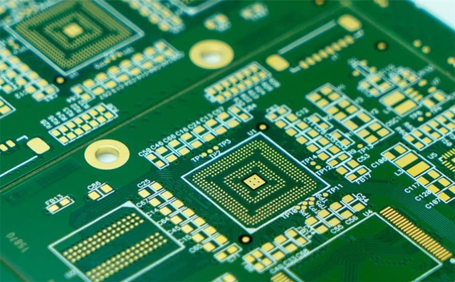
An HDI PCB is a printed circuit board designed to achieve a significantly higher wiring density than conventional PCB technologies. By combining fine-line routing, microvias, blind vias, buried vias, sequential lamination, and high-density component placement, HDI technology allows engineers to integrate more functionality into smaller and thinner electronic products.
Unlike a conventional multilayer PCB that primarily relies on mechanically drilled through-holes, HDI PCB manufacturing makes extensive use of laser-drilled microvias and build-up structures. This enables electrical connections between adjacent layers while preserving valuable routing space.
In practice, HDI technology is not defined simply by the number of PCB layers. Its key characteristics include microvia-based interconnections, fine lines and spaces, high-density routing, and sequential build-up structures.
This guide explains the complete HDI PCB manufacturing process, from initial PCB Design and material selection to fabrication, inspection, testing, and final quality control.
What Is an HDI PCB?
A High-Density Interconnect PCB is a multilayer or build-up circuit board that provides greater interconnection density within a given area than conventional PCB construction.
Typical HDI technologies include:
- Laser-drilled microvias
- Blind vias
- Buried vias
- Sequential lamination
- Fine-line and fine-space routing
- Via-in-pad structures
- Stacked or staggered microvias
- Copper-filled microvias
- High-density component placement
Microvias are typically much smaller than conventional mechanically drilled vias. Their actual dimensions depend on the manufacturer’s process capability, material system, aspect ratio, and design rules. Therefore, a fixed statement such as “microvias are always 50–100 μm” is not appropriate for every HDI process.
HDI technology allows designers to shorten interconnection paths, improve routing efficiency, reduce PCB size, and support increasingly dense semiconductor packages.
HDI PCB Design Stage
The PCB Design stage is one of the most important parts of HDI PCB development. A board can only achieve its intended electrical and mechanical performance when the stackup, routing strategy, materials, vias, thermal design, and manufacturing capabilities are considered together.
A typical HDI design process includes requirements analysis, material selection, schematic development, stackup planning, placement, routing, via design, DFM review, and manufacturing documentation.
1. Define Requirements and Specifications
The first step is to establish the electrical, mechanical, thermal, and manufacturing requirements of the HDI board.
Electrical Requirements
Electrical requirements may include:
- Operating voltage and current
- Controlled impedance
- Signal integrity
- Power integrity
- High-speed interfaces
- Differential-pair requirements
- Crosstalk limitations
- Electromagnetic compatibility
- Ground and power distribution
For high-speed HDI designs, trace geometry and dielectric construction should be coordinated with the target impedance. The designer should not determine trace width from electrical requirements alone; the final geometry also depends on dielectric thickness, copper thickness, dielectric constant, copper roughness, and fabrication tolerances.
Mechanical Requirements
Mechanical specifications typically include:
- Overall PCB dimensions
- Maximum board thickness
- Component height restrictions
- Number of layers
- Mounting-hole locations
- Connector locations
- Bend or flex requirements for rigid-flex designs
- Enclosure constraints
Because HDI technology is often selected to reduce board size, mechanical constraints should be established before detailed routing begins.
Thermal Requirements
Thermal management is particularly important for compact electronics with high power density.
Designers should evaluate:
- Component power dissipation
- Copper distribution
- Thermal vias
- Heat-spreading structures
- Thermal interface materials
- Operating temperature
- PCB material thermal performance
For high-power applications, conventional FR-4 may not always provide sufficient thermal performance, making specialized laminate or metal-backed structures worth considering.
2. HDI PCB Material Selection
Material selection has a direct impact on electrical performance, reliability, thermal behavior, and manufacturability.
FR-4 remains widely used for general-purpose HDI PCBs, but high-speed, RF, flexible, and high-temperature applications may require specialized materials.
| Material | General Characteristics | Electrical Considerations | Thermal / Mechanical Characteristics | Typical Applications |
|---|---|---|---|---|
| FR-4 | Glass-fiber-reinforced epoxy laminate | Moderate Dk/Df; actual values vary by material and frequency | Good mechanical strength and dimensional stability | Consumer electronics, industrial equipment, general HDI |
| Polyimide | Flexible, heat-resistant polymer system | Suitable for flexible and rigid-flex circuits | High flexibility and good thermal stability | Flexible PCB, rigid-flex PCB, high-reliability electronics |
| Rogers RO4000 Series | High-frequency laminate family | Controlled low-loss electrical characteristics depending on grade | Good dimensional and thermal stability | RF, microwave, high-speed applications |
| Taconic RF Materials | High-frequency laminate systems | Low-loss characteristics depending on material grade | Suitable for RF and microwave construction | RF, microwave, antenna circuits |
| Arlon High-Performance Materials | Specialized high-performance laminate systems | Electrical properties vary by grade | Designed for demanding thermal and mechanical environments | Aerospace, high-reliability and high-frequency electronics |
| Megtron Series | High-speed, low-loss laminate family | Low-loss characteristics for high-speed transmission | Designed for demanding signal-integrity applications | Servers, networking, high-speed digital systems |
It is important to use the manufacturer’s actual datasheet values rather than assigning one fixed dielectric constant to an entire material family. Dk and Df can vary with frequency, resin content, glass construction, test method, and material grade.
For HDI production, material selection should also consider laser-drilling performance, resin flow, dimensional stability, copper adhesion, lamination behavior, and compatibility with sequential build-up processes.
3. Schematic Design
Once the specifications and materials have been established, engineers create the circuit schematic using an appropriate EDA or CAD platform.
The schematic defines:
- Electrical connections
- Components
- Power networks
- Ground networks
- Signal interfaces
- Differential pairs
- Critical nets
- Component relationships
Popular PCB design platforms include KiCad, Altium Designer, Cadence Allegro, Siemens Xpedition, and other professional EDA tools.
Before PCB layout begins, the schematic should undergo electrical rule checking (ERC) and engineering review to identify missing connections, incorrect net assignments, unconnected pins, and other potential design problems.
4. HDI PCB Stackup Design
Stackup planning is fundamental to successful HDI PCB Design.
HDI boards may use different layer counts and construction methods depending on the application. For example, a board may use a conventional multilayer core with one or more sequential build-up layers.
A typical HDI stackup may include:
- Signal layers
- Ground planes
- Power planes
- Core materials
- Prepreg or build-up dielectric layers
- Copper foil
The stackup should be electrically and mechanically balanced whenever practical to reduce the risk of warpage during lamination.
For high-speed designs, designers should also consider:
- Reference-plane continuity
- Dielectric thickness
- Controlled impedance
- Differential-pair geometry
- Return-current paths
- Crosstalk
- Via transitions
- Power-distribution performance
A common misconception is that all layers must simply be “adjacent” to prevent EMI. In reality, the objective is to provide appropriate reference planes and controlled return-current paths while maintaining a manufacturable and mechanically stable stackup.
5. Via and Routing Design
Via selection is one of the defining characteristics of HDI technology.
Depending on the stackup and interconnection requirements, designers may use:
- Through vias
- Blind vias
- Buried vias
- Microvias
- Stacked microvias
- Staggered microvias
- Via-in-pad structures
A microvia typically connects adjacent layers or a small number of build-up layers. Laser drilling allows manufacturers to create much smaller via structures than conventional mechanical drilling.
Routing Considerations
HDI routing should consider:
- Trace width
- Trace spacing
- Copper thickness
- Differential-pair spacing
- Controlled impedance
- Return paths
- Via transitions
- Crosstalk
- Current-carrying capacity
- Manufacturing tolerances
Fine-line routing can dramatically increase routing density, but smaller geometry also increases manufacturing sensitivity. Therefore, the designer should establish minimum trace width and spacing according to the actual capabilities of the selected HDI PCB manufacturer.
6. Design for Manufacturing (DFM)
Design for Manufacturing is essential for controlling both yield and production cost.
During the DFM stage, the PCB design is reviewed against manufacturing capabilities and process tolerances.
Important DFM items include:
- Minimum trace width and spacing
- Minimum via diameter
- Microvia geometry
- Pad dimensions
- Solder-mask clearance
- Copper-to-edge clearance
- Hole-to-copper clearance
- Layer registration
- Drill-to-pad alignment
- Via-in-pad requirements
- Copper balancing
- Component spacing
- Panelization requirements
Design Rule Checking (DRC) within the EDA software can automatically identify many violations. However, software DRC alone is not sufficient. A manufacturer-specific DFM review can identify process risks that generic CAD rules may not detect.
This is especially important for HDI because sequential lamination, laser drilling, microvia formation, copper filling, and fine-line fabrication require tighter process control than many conventional PCB structures.
7. Manufacturing Files and Documentation
After the design has been finalized, the engineering team prepares the manufacturing package.
A typical HDI fabrication package may include:
- Gerber files or other fabrication data
- NC drill files
- Drill tables
- Stackup information
- Fabrication drawings
- Solder-mask data
- Silkscreen/legend data
- Surface-finish requirements
- Material specifications
- Controlled-impedance requirements
- Special-process instructions
Gerber files primarily describe PCB layer graphics. Depending on the manufacturing workflow, additional files or structured formats may be required to communicate drill data, stackup information, fabrication specifications, and assembly information.
For complex HDI projects, formats such as ODB++ or IPC-2581 may also be used when a more integrated manufacturing-data package is preferred.
The complete documentation should be reviewed before being released to the manufacturer.
HDI PCB Manufacturing Process
After design approval, the project enters the PCB Manufacturing stage.
HDI fabrication is more complex than conventional PCB production because it may involve sequential lamination, laser drilling, microvia metallization, copper filling, and multiple circuit-forming cycles.
The exact manufacturing sequence varies according to the HDI construction.
1. Core Preparation and Initial Circuit Formation
HDI manufacturing commonly begins with the preparation of the core material.
The core is processed through operations such as:
- Copper surface preparation
- Photoresist application
- Imaging
- Development
- Copper etching
- Resist stripping
- Inspection
The result is the required circuit pattern on the core layers.
The actual sequence may vary depending on whether the board uses conventional multilayer construction, 1+N+1 HDI, 2+N+2 construction, or more advanced any-layer HDI structures.
2. Photoresist Application and Imaging
A photoresist is applied to the copper surface and patterned using an imaging process.
The exposed and unexposed regions are developed according to the type of photoresist and imaging process. Modern PCB factories may use laser direct imaging (LDI) instead of traditional phototools for greater registration accuracy and finer geometries.
The imaging process determines the circuit pattern that will subsequently be etched or plated.
For HDI manufacturing, imaging accuracy is particularly important because fine lines and small pads provide less process margin than conventional PCB geometries.
3. Copper Etching
After imaging and development, unwanted copper is removed through a controlled chemical etching process.
The remaining copper forms the required circuit pattern.
Etching must be tightly controlled because excessive or insufficient etching can alter:
- Trace width
- Trace spacing
- Pad dimensions
- Fine-line geometry
- Impedance characteristics
HDI production therefore requires close control of chemical concentration, temperature, spray pressure, conveyor speed, and other process parameters.
4. Automated Optical Inspection (AOI)
After circuit formation, Automated Optical Inspection is used to compare the manufactured circuit pattern against the intended design data.
AOI can identify potential defects such as:
- Open circuits
- Short circuits
- Missing copper
- Excess copper
- Trace-width abnormalities
- Pad defects
- Pattern deviations
AOI does not replace every other form of testing, but it provides an important manufacturing-process checkpoint before the board proceeds to subsequent operations.
5. Sequential Lamination
Sequential lamination is one of the most important processes in many HDI structures.
Instead of laminating every layer in one conventional operation, additional dielectric and copper layers are built onto an existing multilayer core through one or more sequential cycles.
During lamination:
- Dielectric material is placed between conductive layers.
- Heat softens and cures the resin system.
- Pressure consolidates the stack.
- Registration between layers is controlled.
- The dielectric thickness is established.
The actual lamination temperature and pressure are material- and process-dependent. Therefore, fixed values such as 190°C and 275–400 psi should not be treated as universal HDI manufacturing requirements.
The manufacturer selects a lamination profile based on the laminate, prepreg, copper pattern, resin system, board thickness, and equipment.
6. Laser Drilling of Microvias
Laser drilling is a defining process in many HDI PCB manufacturing flows.
UV or CO₂ laser systems can be used depending on the material stackup and manufacturing requirements.
Laser drilling creates microvias that provide short interconnections between adjacent or nearby layers.
The process must control:
- Via diameter
- Depth
- Registration
- Laser energy
- Dielectric thickness
- Bottom copper condition
- Hole-wall quality
Because microvias are extremely small, laser drilling requires accurate positioning and process control.
7. Microvia Metallization and Copper Plating
After drilling, the microvia must be metallized so that it can electrically connect the required copper layers.
A typical process can include:
- Desmear or surface conditioning
- Chemical copper deposition
- Electrolytic copper plating
- Microvia filling when required
- Surface treatment and inspection
Copper-filled microvias are particularly useful for via-in-pad structures and stacked microvia construction.
The copper-plating process must provide adequate electrical continuity, mechanical reliability, and resistance to thermal cycling.
8. Additional Build-Up Cycles
For advanced HDI structures, additional dielectric and copper layers may be added after the first build-up cycle.
The process may then repeat:
Lamination → Laser Drilling → Desmear → Metallization → Copper Plating → Circuit Formation
The number of cycles depends on the required HDI construction.
For example, advanced designs may use stacked or staggered microvias to connect several build-up layers without relying exclusively on large through-hole structures.
This build-up capability enables extremely dense interconnections in compact electronic products.
9. Drilling and Via Formation
Mechanical drilling is still used in HDI PCBs where larger holes are required.
Depending on the design, the board may contain:
- Through-holes
- Mechanical blind vias
- Buried vias
- Laser microvias
Mechanical drilling and laser drilling serve different purposes and may be combined in the same PCB.
For high-speed designs, unnecessary via stubs should be minimized because long unused portions of vias can introduce parasitic effects and signal-integrity problems.
10. Solder Mask Application
After the circuit structure has been completed, solder mask is applied to protect exposed copper areas and reduce the risk of solder bridging between adjacent conductors.
The process generally includes:
- Surface cleaning and preparation
- Solder-mask coating
- Imaging
- Development
- Curing
- Inspection
The green appearance commonly associated with PCBs comes from the solder-mask system, not from the copper itself or the fiberglass substrate.
Although green is widely used, HDI PCBs can also be manufactured with black, blue, red, white, yellow, and other solder-mask colors.
11. Surface Finish
A surface finish is applied to exposed copper pads to improve solderability and protect the copper surface from oxidation.
Common PCB surface finishes include:
- ENIG (Electroless Nickel Immersion Gold)
- ENEPIG (Electroless Nickel Electroless Palladium Immersion Gold)
- HASL
- Lead-free HASL
- OSP
- Immersion tin
- Immersion silver
The appropriate finish depends on soldering requirements, component pitch, storage requirements, reliability expectations, cost, and application environment.
For fine-pitch HDI components, finishes that provide a relatively flat surface can be advantageous for assembly.
12. Electrical Testing
Electrical testing is performed to verify that the manufactured board conforms to the intended circuit connectivity.
Typical electrical tests include:
Continuity Testing
Continuity testing verifies that required electrical paths are properly connected.
Isolation Testing
Isolation testing checks that conductors that should remain electrically separated do not create unintended connections.
Flying-Probe Testing
Flying-probe testers can be useful for prototypes and lower-volume production because they can test boards without requiring a dedicated fixture.
Fixture-Based Testing
For higher-volume production, dedicated fixtures may be used to perform faster electrical testing.
The appropriate test method depends on production volume, PCB complexity, test coverage, and customer requirements.
13. Final Inspection and Quality Control
Electrical testing is only one part of the final inspection process.
A comprehensive HDI PCB quality-control program may include:
- AOI
- Dimensional inspection
- Microsection analysis
- X-ray inspection when applicable
- Solder-mask inspection
- Surface-finish inspection
- Plated-hole inspection
- Microvia inspection
- Electrical testing
- Impedance testing for controlled-impedance designs
- Visual inspection
For demanding applications, test coupons may also be manufactured alongside production panels to verify characteristics such as impedance, plating quality, and other critical process parameters.
Key Advantages of HDI PCB Technology
HDI technology provides several important benefits for modern electronics.
Higher Routing Density
Microvias and fine-line structures allow more electrical connections to be routed within a limited PCB area.
Smaller PCB Size
HDI construction can reduce the space required for interconnections, helping engineers develop smaller electronic products.
Better Component Integration
Fine-pitch packages and high-density components can be integrated more effectively using structures such as microvias and via-in-pad.
Improved High-Speed Interconnect Performance
Shorter electrical paths and optimized via structures can reduce parasitic effects and support better signal-integrity performance when properly designed.
Greater Design Flexibility
Build-up layers allow designers to add routing capacity where it is needed without necessarily increasing the entire board thickness or relying on conventional through-hole structures.
Common HDI PCB Applications
HDI PCBs are widely used in applications where size, functionality, interconnection density, and reliability are important.
Typical applications include:
Smartphones and Wearable Electronics
Compact consumer devices require high component density and extremely efficient PCB routing.
Medical Electronics
Medical devices often require compact, reliable electronics for imaging, monitoring, diagnostic, and portable equipment.
Automotive Electronics
Advanced driver-assistance systems, infotainment systems, cameras, sensors, and control modules can benefit from HDI technology.
Networking and Communication Equipment
High-speed communication systems require controlled impedance, dense routing, and reliable multilayer interconnections.
Aerospace and Defense Electronics
Compact and highly integrated electronics can use advanced HDI construction when the design and manufacturing requirements justify it.
Industrial and IoT Devices
Industrial controllers, sensors, gateways, and connected devices increasingly require compact electronics with higher functional density.
HDI PCB Manufacturing Challenges
Despite its advantages, HDI fabrication requires tighter process control than many conventional PCB technologies.
Common challenges include:
- Layer-to-layer registration
- Microvia reliability
- Copper filling quality
- Fine-line etching
- Sequential-lamination accuracy
- Resin flow control
- Warpage
- Thermal stress
- Material compatibility
- Yield management
- Manufacturing cost
One particularly important issue is microvia reliability. Because microvias can experience significant mechanical and thermal stresses during assembly and operation, their construction must be carefully designed and manufactured.
For this reason, designers should involve the PCB manufacturer early in the development process rather than waiting until the design is completely finished.
How to Choose an HDI PCB Manufacturing Partner
Selecting an HDI manufacturing partner requires more than comparing unit prices.
Consider the manufacturer’s capabilities in:
- Laser drilling
- Microvia metallization
- Copper-filled microvias
- Sequential lamination
- Fine-line fabrication
- High-density registration
- Controlled impedance
- AOI and electrical testing
- X-ray and microsection analysis
- Prototype and volume production
It is also important to verify whether the supplier’s actual process window supports the trace widths, spacing, microvia dimensions, stackup, material system, and tolerances specified in the design.
For complex HDI projects, early DFM collaboration can help identify manufacturability risks before tooling and mass production begin.
HDI PCB Manufacturing with Kingda
A reliable HDI manufacturing partner should be capable of supporting the entire process from engineering review and DFM analysis to fabrication, inspection, and electrical testing.
Kingda can support customers with PCB engineering and manufacturing requirements involving high-density interconnect structures, multilayer construction, fine-line routing, microvias, controlled impedance, surface finishes, and PCB quality inspection.
By coordinating PCB Design requirements with actual PCB Manufacturing capabilities at an early stage, engineers can reduce unnecessary redesigns, improve manufacturing yield, and achieve a more reliable final product.
For demanding HDI applications, the most effective approach is to establish the manufacturing capability, material system, stackup, via structure, and critical tolerances before finalizing the PCB design.
Conclusion
HDI technology has become an important solution for modern electronics that require greater functionality in smaller spaces. Through microvias, blind and buried vias, fine-line routing, sequential lamination, and build-up structures, HDI PCB technology enables designers to achieve substantially higher interconnection density than many conventional PCB constructions.
However, successful HDI production depends on close coordination between PCB Design and PCB Manufacturing. Stackup selection, material properties, impedance requirements, via structures, routing geometry, thermal management, DFM rules, and manufacturing tolerances must all be considered as part of one integrated process.
From schematic development and stackup planning to laser drilling, sequential lamination, copper plating, solder-mask application, surface finishing, and electrical testing, every stage contributes to the reliability and performance of the finished PCB.
For compact smartphones, medical equipment, automotive electronics, networking systems, and other advanced electronic products, choosing an experienced HDI PCB manufacturing partner can help transform a high-density design into a manufacturable and reliable product.