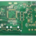
High Frequency PCB for Mobile Devices: 2026 Price Guide
What High Frequency Boards Cost and Why
Modern mobile devices are packed with radios. 5G smartphones, tablets, wearables and wireless modules all depend on a high frequency pcb that carries RF signals with low loss and controlled impedance. These boards cost more than ordinary ones, and the difference is not markup: it is materials, microvia processes and RF design discipline. This guide breaks down 2026 pricing for high frequency PCBs in mobile devices, explains every major cost driver, compares material costs and shows how to reduce expense without sacrificing radio performance.
What Is a High Frequency PCB for Mobile Devices?
A high frequency pcb is a circuit board engineered for signals from about 500 MHz to 2.4 GHz and beyond, common in communication and high-speed RF equipment. Typical applications inside mobile products include 5G communication modules, WiFi and Bluetooth modules, RF antennas, power amplifiers and filter circuits, mobile data and communication systems, and wearable terminals. Instead of ordinary FR-4, these boards use Rogers, PTFE or low-loss polyimide laminates that hold a stable dielectric constant and keep dielectric loss low, which is exactly what RF circuits need.
Core Factors That Drive High Frequency PCB Price
The price of a high frequency pcb depends on a set of engineering variables. Substrate and dielectric material choice is the largest one, since RF-grade laminates cost several times more than standard FR-4. Layer count and stack-up structure matter because mobile RF boards commonly run four to sixteen layers with HDI features. RF trace routing rules add design and inspection effort, and microvia, blind and buried via processing requires laser drilling and multiple lamination cycles. Finally, impedance testing, shielding and RF qualification add measurable cost to every batch.

Material Cost Comparison
Material expense dominates the price difference between RF and standard boards. As a 2026 reference, Rogers 5880 and 4350 laminates run about USD 90-220 per square meter, PTFE-based materials USD 120-260, low-loss polyimide USD 60-160, and FR-4 hybrid stack-ups only USD 30-80. The engineering guidance that follows is straightforward: Rogers and PTFE belong in the most demanding RF sections, while FR-4 with high-frequency hybrid layers is the most economical route when performance allows it.
Price Ranges by Mobile Application
Different products land in different price bands. Smartphone boards typically cost USD 15-40, smartwatches USD 15-40, wearables USD 10-50, IoT handheld devices USD 25-70, and 5G modules USD 40-110 per board. Most of these designs use four to sixteen layer HDI construction with microvias and shielding structures, which is why the prices sit well above standard consumer PCB levels. The radio budget of the product, not the board area, usually decides where in the range a design falls.
Design Challenges in Small Mobile Devices
Packing RF into a thin smartphone or a coin-sized wearable creates problems that board design must solve early. Antenna clearance is limited, so the RF section needs precise stack-up placement and grounded keep-out zones. Several radios coexist in one device, which demands isolation between WiFi, Bluetooth, GPS and cellular paths to stop desense. Thin enclosures remove heat slowly, so power amplifiers and charging circuits need thermal vias and copper spreading. Shielding cans add cost but are often the only reliable answer for noise-sensitive receivers. A factory with real mobile RF experience can flag these issues during DFM review before tooling, saving the expensive re-spin cycles that plague first-time RF designs.
How to Reduce High Frequency PCB Cost
Cost reduction is possible without compromising RF performance. Hybrid stack-up design limits expensive laminates to critical layers. Routing and impedance optimization can shrink layer count. Reducing unnecessary HDI layers removes laser via and lamination steps, and alternative materials such as polyimide can replace PTFE where loss requirements allow. Early engineering cooperation with the factory also helps, because a correct stack-up review prevents expensive re-spins. The combination typically cuts 15-30 percent from a first-quote price while keeping radio performance intact.
High Frequency vs Ordinary PCB Pricing
Why does a high frequency pcb cost two to four times more than a standard board? The reasons are concrete: tighter control of dielectric constant and loss, laser drilling and microvia processing, high-frequency routing rules, and the shielding, testing and impedance matching that RF designs require. Each of those steps adds process time and inspection depth. When a product genuinely needs RF performance, the premium is unavoidable; the job of the engineer is to avoid paying it on layers that do not carry high-frequency signals.
Manufacturing Technology Requirements
RF-capable factories must hold a defined set of capabilities. Typical parameters include minimum line width of 0.05-0.1 mm, HDI architectures such as 1+N+1 and 2+N+2, impedance control within plus or minus 5 percent, support for microvias and blind or buried vias, and repeated lamination cycles. These capabilities directly determine RF performance and signal integrity in mobile devices, so supplier audits should ask for proof of each one rather than a general marketing claim.

Testing and Qualification Steps
RF boards need verification that digital boards never see. Impedance verification on controlled traces should be measured by TDR and reported per panel. Microsection analysis confirms via and microvia quality after lamination. Insertion loss and return loss checks validate the material and routing decisions on high-speed links. On assembled modules, antenna matching and over-the-air testing prove real-world performance, and certification support for standards such as FCC and CE closes the loop. These tests add lead time and cost, but they are the difference between a mobile product that passes certification on the first attempt and one that burns three months in rework.
Choosing a High Frequency PCB Supplier
Selection should start with engineering capability, not price. Confirm the factory can hold impedance tolerances, has experience with Rogers, PTFE and hybrid stack-ups, and can run the HDI and microvia processes your design needs. Then verify prototype speed and volume stability on the same process, and ask whether PCB manufacturing can be paired with PCBA testing for assembled RF modules. RF work benefits from a single responsible partner, because board material, assembly and antenna tuning interact strongly.
Working With a Specialist Manufacturer
A specialist such as gopcb keeps RF-grade materials in stock, supports HDI and multilayer builds for mobile modules, and offers impedance testing with RF debugging on assembled boards. When the factory also provides PCB design and layout review and SMT assembly, the engineering loop from stack-up to shipped module stays under one quality system, which shortens development cycles for 5G and wireless products.
High Frequency PCB FAQ
Q1: Why are high frequency PCBs more expensive? RF-grade materials, microvia processing, impedance control and RF testing all cost more than standard fabrication.
Q2: Which materials are best for mobile RF boards? Rogers and PTFE for critical RF layers, with polyimide or FR-4 hybrids as economical alternatives where loss allows.
Q3: How much does a smartphone high frequency pcb cost? Typically USD 15-40 depending on layer count and HDI structure.
Q4: Can cost be reduced without hurting performance? Yes, through hybrid stack-ups, routing optimization and reduced HDI layers, with early DFM review.
Conclusion
The high frequency pcb is the quiet enabler of everything wireless in mobile products. Its cost is driven by real engineering requirements, from exotic laminates to microvia precision, but disciplined design keeps that cost where it belongs. By matching materials to the actual RF budget and working with a factory that holds genuine high-frequency capability, mobile OEMs get boards that pass certification and perform in the field without paying for unnecessary performance.