How to Etch a PCB: PCB Design & PCB Manufacturing Guide
You have successfully tested your circuit on a breadboard. What comes next?
Whether you are a hobbyist, student, or engineer, transferring a working circuit from a breadboard to a printed circuit board (PCB) is a logical next step if you want your project to become more compact, professional, durable, and reliable.
A PCB is an insulating substrate with conductive copper features that electrically connect components. These conductive features include traces, pads, and planes. When making a PCB yourself, one of the basic tasks is to selectively remove unwanted copper while preserving the copper traces that form the circuit.
This is where PCB etching comes in.
During the PCB etching process, a circuit pattern is first transferred onto a copper-clad board. The exposed copper is then chemically removed by an etchant, while the protected areas remain intact and become the conductive pattern of the finished board.
After etching, the board can be cleaned, drilled, inspected, and prepared for through-hole component installation or other assembly steps. Although home PCB etching is suitable for simple prototypes and educational projects, professional PCB Manufacturing typically uses controlled imaging, etching, plating, drilling, solder mask, surface finishing, electrical testing, and inspection processes to achieve higher consistency and reliability.
This guide explains how to etch a PCB, focusing on the commonly used toner-transfer method for DIY PCB fabrication.
PCB Layout Transfer Methods
Before starting the etching process, you need to transfer the PCB layout onto the copper-clad board. The transferred pattern acts as an etch-resistant mask that protects the copper traces you want to keep.
Several methods can be used to transfer a PCB Layout, including:
- Toner transfer
- Photoresist and UV exposure
- Direct imaging
- CNC milling or isolation routing
- Laser-based processing
For simple DIY projects, toner transfer is one of the most accessible approaches because it requires relatively inexpensive equipment.
However, toner transfer is not as precise or repeatable as professional PCB imaging processes. Fine-pitch components, narrow traces, small clearances, and complex multilayer designs generally require professional manufacturing equipment.
PCB Etching Using the Toner Transfer Method
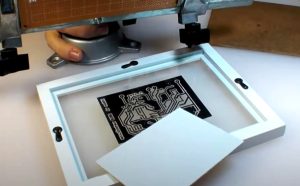
Toner transfer is popular among beginners because it allows a PCB pattern to be transferred using a laser printer and heat.
If you are learning how to etch a PCB, the following equipment and materials may be required:
- Copper-clad PCB laminate
- Laser printer
- Glossy paper or dedicated toner-transfer paper
- Laminator or temperature-controlled heat-transfer equipment
- Suitable PCB etchant
- Plastic or chemically compatible tray
- Fine abrasive pad or fine sandpaper
- Cleaning materials
- Chemical-resistant gloves
- Safety goggles
- Appropriate ventilation
A properly controlled process is important because poor surface preparation, incorrect transfer temperature, or inaccurate printing can result in broken traces and unwanted copper remaining on the board.
Step 1: Design and Print the PCB Layout
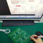
Start by creating the circuit and PCB Design using an appropriate ECAD tool such as KiCad, EasyEDA, or another PCB design platform.
The general workflow is:
- Create the schematic.
- Assign appropriate footprints.
- Create the PCB layout.
- Check component placement and routing.
- Run design-rule checks.
- Generate the required artwork for the toner-transfer process.
- Print the pattern at its intended physical scale.
The printed artwork must maintain accurate dimensions. Make sure the printer is configured to print at 100% scale or actual size, rather than “Fit to Page.”
Whether the artwork should be mirrored depends on which PCB surface and transfer method you are using. For toner transfer, the artwork is commonly mirrored so that the transferred copper pattern has the correct orientation. Always verify the orientation with your specific transfer process before printing.
Before proceeding, check:
- Board dimensions
- Trace width
- Clearance
- Pad size
- Hole locations
- Component orientation
- Text orientation
- Layer selection
A small printing or mirroring error can make the final PCB unusable.
Step 2: Prepare the Copper-Clad Board
Cut the copper-clad laminate to the required size.
Then carefully clean the copper surface to remove:
- Oxidation
- Dust
- Grease
- Fingerprints
- Other contaminants
A fine abrasive pad or fine sandpaper can be used to lightly prepare the surface. Avoid excessively scratching the copper because deep scratches can affect toner transfer.
After cleaning, handle the board by its edges to avoid transferring oil from your fingers back onto the copper surface.
A clean copper surface is one of the most important factors affecting toner adhesion.
Step 3: Transfer the Toner
Place the printed artwork against the prepared copper surface according to the selected transfer method.
Apply controlled heat and pressure using a laminator or suitable heat-transfer equipment. If a household iron is used for a DIY process, maintain consistent pressure and temperature and follow the transfer-paper manufacturer’s instructions.
The objective is to transfer the toner evenly onto the copper.
After the transfer is complete:
- Allow the board to cool.
- Soak it in water if required by the paper-transfer method.
- Carefully remove the paper.
- Inspect the transferred toner pattern.
The copper traces should be completely covered by toner.
Look carefully for:
- Broken traces
- Pinholes
- Missing pads
- Unwanted toner
- Shorted traces
- Incorrect dimensions
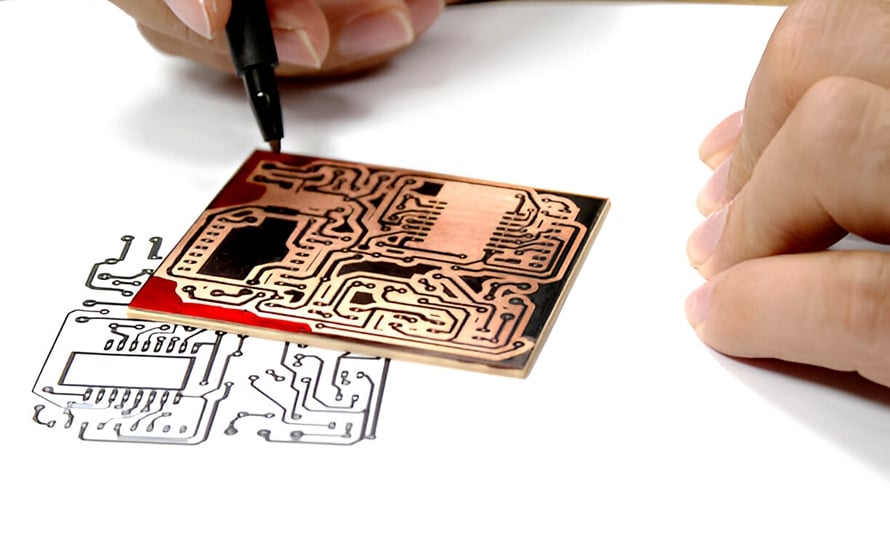
Small defects can sometimes be corrected manually with an appropriate etch-resistant marker before etching.
Step 4: Etch the PCB
Once the toner pattern has been verified, place the board into a suitable etchant.
The etchant removes exposed copper while the toner protects the areas that will become the circuit traces.
During the process:
- Place the PCB into a chemically compatible container.
- Follow the etchant manufacturer’s instructions for concentration and temperature.
- Ensure the copper surface is properly exposed to the solution.
- Gently agitate the solution if recommended.
- Monitor the exposed copper as it is removed.
- Remove the board once the unwanted copper has been sufficiently etched.
- Rinse the PCB thoroughly with water according to the chemical manufacturer’s instructions.
Do not leave the board in the etchant longer than necessary. Excessive etching can cause undercutting, where the chemical attacks copper underneath the protective pattern and reduces the effective trace width.
After rinsing, inspect the copper pattern carefully.
Step 5: Clean and Finish the PCB
After etching, remove the remaining toner using a suitable cleaning method recommended for the transfer material.
Once the copper traces are exposed, inspect the board for:
- Incomplete etching
- Over-etching
- Broken traces
- Short circuits
- Insufficient clearance
- Damaged pads
If the design requires through-hole components, drill the appropriate component holes using suitable PCB drilling equipment.
For a more complete DIY board, additional finishing processes may include solder mask application and surface protection. However, applying a professional-quality solder mask at home is considerably more difficult than applying toner and should be treated as a separate process.
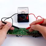
Before assembly, verify electrical continuity and check for unintended shorts.
PCB Etchant: How to Choose the Right Etchant
Choosing an appropriate etchant is an important part of PCB Fabrication.
Different chemicals provide different etching rates, handling requirements, waste characteristics, and process control requirements.
Commonly encountered PCB etchants include ferric chloride and ammonium persulfate. Other chemical systems may also be used in PCB manufacturing, but some require substantially greater chemical-handling expertise and ventilation.
| Etchant | Typical Characteristics | Advantages | Considerations |
|---|---|---|---|
| Ferric chloride | Moderate etching rate | Widely available and commonly used for DIY PCB etching | Can stain surfaces and clothing; requires appropriate waste handling |
| Ammonium persulfate | Moderate etching rate | Relatively clean appearance and easy visual monitoring | Strong oxidizing chemical; requires careful handling |
| Cupric chloride systems | Can provide controlled industrial etching | Can be regenerated in controlled processes | Chemical preparation, ventilation, and process control are important |
| Household acid/salt mixtures | Generally slow and inconsistent | Low-cost materials may be accessible | Poor process control and unsuitable for fine PCB features |
Chemical performance depends on concentration, temperature, agitation, copper loading, and process conditions. Therefore, simply comparing etchants by nominal etching speed does not provide a complete picture.
Which PCB Etchant Should You Choose?
For simple DIY PCB projects, ferric chloride and ammonium persulfate are commonly encountered options.
Ferric chloride is widely used for hobbyist PCB etching and is relatively easy to obtain, but it can leave stubborn stains.
Ammonium persulfate provides a cleaner-looking process and can make it easier to observe the copper being removed, but it still requires appropriate chemical handling and protective equipment.
For beginners, the most important consideration is not simply etching speed. Choose a process with clear manufacturer instructions, appropriate ventilation, suitable containers, and a practical waste-disposal method.
For commercial PCB Manufacturing, manufacturers normally use controlled chemical processes rather than improvised household mixtures. These processes are designed to maintain consistent trace geometry, copper thickness, production throughput, and environmental controls.
Common Problems During PCB Etching
Even when the basic process appears straightforward, DIY PCB etching can produce inconsistent results.
Over-Etching
Over-etching occurs when the board remains in the chemical solution too long or the process is too aggressive. It can reduce trace width and damage fine features.
Under-Etching
Under-etching occurs when exposed copper is not completely removed. This can leave unwanted copper bridges between adjacent traces and cause electrical shorts.
Poor Toner Transfer
If the copper surface is dirty or the transfer temperature and pressure are inappropriate, the toner may not adhere properly.
The result can include:
- Missing traces
- Broken pads
- Pinholes
- Uneven line widths
Incorrect PCB Scaling
If the artwork is printed with automatic scaling enabled, the physical dimensions may differ from the original PCB Design.
This can cause serious problems with:
- Component footprints
- Connector spacing
- Mounting holes
- Board dimensions
- Through-hole component alignment
Always verify the printed dimensions before transferring the artwork.
Insufficient Clearance
DIY etching cannot reproduce arbitrarily fine traces and spacing. A design that works well on a professional PCB fabrication line may not transfer reliably using a home toner-transfer process.
For beginners, relatively generous trace widths and clearances are easier to reproduce consistently.
PCB Etching Safety Guidelines
Safety should be the highest priority when working with PCB etchants, solvents, heat, and drilling equipment.
Follow these basic precautions:
- Wear chemical-resistant gloves suitable for the chemicals being used.
- Wear appropriate safety goggles to protect your eyes from splashes.
- Wear protective clothing or an apron.
- Work in a well-ventilated area appropriate for the chemicals involved.
- Keep food, beverages, and cooking equipment away from the workspace.
- Do not use kitchen containers or utensils for chemical processing.
- Follow the chemical manufacturer’s Safety Data Sheet (SDS).
- Never pour used etchant into a sink unless local regulations and the chemical instructions explicitly permit it.
- Collect and dispose of chemical waste according to applicable local requirements.
- Keep children and pets away from the work area.
- Wash your hands thoroughly after completing the process.
- Handle heat-transfer equipment and drilling tools carefully.
Different etchants have different hazards, so always follow the specific handling and disposal instructions for the chemical you are using.
A safe workspace is an essential part of successful PCB Manufacturing and DIY PCB fabrication.
DIY PCB Etching vs. Professional PCB Manufacturing
DIY etching is useful for learning basic PCB fabrication and producing simple prototypes, but it has important limitations.
| Factor | DIY PCB Etching | Professional PCB Manufacturing |
|---|---|---|
| Typical application | Education, hobby projects, simple prototypes | Prototypes, production, commercial electronics |
| Layer count | Usually single or simple double-sided boards | Single-sided to advanced multilayer PCBs |
| Trace precision | Limited by transfer process | Controlled according to manufacturing capability |
| Vias | More difficult to implement reliably | Standard manufacturing capability |
| Plated through-holes | Limited or unavailable in basic DIY processes | Standard production process |
| Solder mask | Optional/manual | Professionally controlled |
| Surface finish | Basic or DIY-applied | HASL, ENIG, OSP, immersion tin, etc. |
| Electrical testing | Usually manual | Automated and/or fixture-based testing |
| Repeatability | Highly process-dependent | Controlled production process |
| Production volume | Very limited | Prototype to mass production |
Professional PCB fabrication involves much more than simply removing unwanted copper. Depending on the design, manufacturers may use multilayer lamination, precision drilling, copper plating, imaging, solder mask, surface finishing, silkscreen, automated inspection, electrical testing, and other controlled processes.
For commercial products, working with an experienced manufacturer such as Kingda can help bridge the gap between a tested prototype and a manufacturable PCB.
How PCB Design Affects Etching Results
Successful PCB Design is closely connected to manufacturability.
Before creating a DIY etched PCB, consider:
- Minimum trace width
- Minimum spacing
- Pad dimensions
- Hole diameter
- Board outline
- Copper area
- Component package size
- Connector locations
- Thermal requirements
- Electrical clearance
- Manufacturing tolerance
A PCB that is easy to manufacture is generally easier to prototype and troubleshoot.
For professional production, the design should also follow the manufacturer’s Design for Manufacturability (DFM) requirements. Trace/space capability, hole sizes, copper thickness, layer stackup, solder mask clearance, and surface finish should be reviewed before fabrication.
When Should You Use DIY PCB Etching?
DIY PCB Etching can be appropriate when:
- You want to learn PCB fabrication.
- You need a simple prototype.
- The circuit uses relatively large features.
- You are working on an educational project.
- You want to experiment with PCB layout and fabrication.
- Production-level reliability is not required.
Professional PCB Manufacturing is generally more appropriate when the board requires:
- Fine-pitch components
- HDI structures
- Multilayer construction
- Controlled impedance
- Plated through-holes
- Reliable vias
- Tight dimensional tolerances
- Controlled surface finishes
- High production consistency
- Electrical testing
- Commercial or safety-critical reliability
Conclusion
Learning how to etch a PCB is an excellent way to understand the fundamentals of PCB fabrication. The toner-transfer method can provide a relatively accessible introduction to transferring a circuit pattern, removing unwanted copper, drilling the finished board, and checking the resulting electrical connections.
However, DIY PCB etching has clear limitations. Trace accuracy, undercutting, vias, plated holes, solder mask, surface finish, multilayer structures, and production repeatability are difficult to control using basic home equipment.
For simple educational projects and prototypes, DIY etching can provide valuable hands-on experience. For commercial electronics, complex designs, and applications requiring consistent quality, professional PCB Manufacturing provides a much more controlled production environment.
From PCB Design and DFM review to fabrication, PCB Assembly, inspection, and testing, a complete manufacturing process helps transform a working prototype into a reliable electronic product. Kingda can serve as a manufacturing partner when a PCB project needs to move beyond DIY prototyping toward professional production.