How to Output Gerber Files Correctly: A Complete Guide for PCB Engineers
When a PCB design is completed, the design files must be converted into production-ready manufacturing data before the board can be fabricated. Among all manufacturing data formats, Gerber Files remain one of the most widely used formats for PCB fabrication.
The three commonly used PCB design platforms include Cadence Allegro, PADS, and Altium Designer. While each software platform has its own advantages, PCB manufacturers generally prefer receiving standardized Gerber and drill files rather than relying directly on native design files.
Sending the original PCB design file to a manufacturer may create unnecessary risks, including software-version compatibility issues, missing design elements, incorrect settings, or manufacturing data discrepancies. Preparing and checking the Gerber package before production can significantly reduce these risks.
For engineers working on prototypes or production boards, a properly prepared manufacturing package is an important part of reliable PCB Manufacturing.
Why Should Engineers Output Gerber Files Before PCB Production?
Although PCB manufacturers may support native files from Altium Designer, PADS, or other design software, sending standardized production files is generally safer.
A complete Gerber package allows the manufacturer to independently interpret each manufacturing layer without depending on the original CAD software environment.
Before sending files to a PCB manufacturer, engineers should:
- Verify the PCB design version.
- Confirm the copper layer configuration.
- Check solder mask openings.
- Verify board outline and routing.
- Confirm drill sizes and drill types.
- Generate Gerber files.
- Generate NC Drill files.
- Import the output files into CAM software for verification.
Spending a few minutes checking the exported files can help identify missing layers, incorrect apertures, wrong drill sizes, or manufacturing data errors before production begins.
For complex boards, professional PCB Design and manufacturing review can further reduce fabrication risks.
How to Output Gerber Files in Altium Designer
The following procedure describes a practical workflow for preparing Gerber and drill files using Altium Designer.
1. Check Via Solder Mask Settings
If your design requires vias to be covered by solder mask, verify the via solder mask settings before generating the production files.
In Altium Designer, select the appropriate vias and review their solder mask properties. Depending on the manufacturing requirement, vias can either be covered with solder mask or exposed through solder mask openings.
This setting should be confirmed before Gerber generation because solder mask information is included in the corresponding Gerber layer.
For example, engineers should verify:
- Top solder mask openings
- Bottom solder mask openings
- Via tenting requirements
- Component pad openings
- Special exposed copper areas
An incorrect solder mask configuration can result in unexpected exposed vias or missing openings on the manufactured PCB.
2. Add a Drill Table
A drill table provides a convenient way to verify hole sizes and hole types before manufacturing.
Place the drill table outside the PCB outline or in another suitable area of the design. It should clearly identify the drill sizes used in the PCB.
The drill information can be used to cross-check:
- Plated through holes
- Non-plated through holes
- Via hole sizes
- Component lead holes
- Mechanical holes
- Hole quantities
Modern versions of Altium Designer provide dedicated drill-table functions, making it easier to review the drilling information before exporting production files.
This step is particularly important for boards containing multiple drill sizes because incorrect drill data can directly affect component assembly and mechanical compatibility.
3. Generate Gerber Files
The production output normally consists of two major categories:
- Gerber files
- NC Drill files
Gerber files contain the graphical manufacturing information for the PCB, while NC Drill files provide the drilling data required to manufacture the holes.
In Altium Designer, open the PCB project and select the Gerber output function under the File menu.
Recommended Gerber Settings
When configuring the Gerber output, review the following settings:
- Units
- Format
- Coordinate precision
- Used layers
- Apertures
- Solder mask layers
- Silkscreen layers
- Mechanical layers
- Board outline
A commonly used configuration is an imperial format with sufficient coordinate precision, such as 2:5. However, the final format should always be consistent with the requirements of the PCB manufacturer.
For layer selection, selecting the layers actually used by the PCB helps prevent unnecessary manufacturing files while ensuring that all required layers are included.
Typical Gerber outputs may include:
- Top Copper
- Bottom Copper
- Inner Copper Layers
- Top Solder Mask
- Bottom Solder Mask
- Top Silkscreen
- Bottom Silkscreen
- Board Outline
- Additional mechanical or fabrication layers when required
After reviewing the settings, generate the Gerber package.
4. Generate NC Drill Files
Gerber files alone are not sufficient for PCB manufacturing because they do not normally contain all of the drilling information required by the fabrication process.
Therefore, an NC Drill Files package should also be generated.
In Altium Designer, open the NC Drill output function and configure the units and coordinate format to match the Gerber files.
Before exporting, verify:
- Drill units
- Coordinate format
- Plated hole information
- Non-plated hole information
- Drill sizes
- Hole quantities
The Gerber and NC Drill files should use compatible coordinate systems and units. A mismatch between these files can result in incorrect hole positions or manufacturing errors.
5. Organize the Manufacturing Package
After exporting the production data, place the Gerber and NC Drill files in a dedicated project folder.
A typical manufacturing package may contain:
- Gerber files
- NC Drill files
- Board outline
- Readme or fabrication notes
- Drill table
- Assembly documentation when required
- BOM and pick-and-place files for PCBA projects
If the manufacturer does not specifically require the native PCB design file, it is generally better to provide the complete manufacturing package rather than relying on the original CAD file.
For prototype projects, a well-organized production package can also simplify communication between the engineering and manufacturing teams. This is especially useful when moving from PCB Prototype development to subsequent production stages.
How to Check Gerber Files Before Manufacturing
Generating the files is only the first step. Engineers should also verify the exported files before sending them to the manufacturer.
A simple and effective method is to import the generated files into Altium Designer’s CAM environment.
1. Create a CAM Document
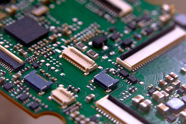
Open Altium Designer and create a new CAM document.
Then use the Gerber import function to load the exported Gerber files.
Import all relevant layers and check whether the PCB appears correctly.
2. Import the NC Drill Files
After importing the Gerber files, import the corresponding NC Drill files into the same CAM document.
The drill holes should align correctly with the PCB pads, vias, and other features.
At this stage, engineers should carefully inspect the entire board.
3. Check the PCB Layer Stack
Verify that every required layer has been exported.
Check for:
- Missing copper layers
- Missing solder mask layers
- Missing silkscreen
- Incorrect board outline
- Incorrect mechanical layers
- Unexpected empty layers
For multilayer boards, pay particular attention to the sequence of internal copper layers.
4. Check the Board Outline
The board outline is one of the most important manufacturing elements.
Make sure the PCB shape is complete and closed.
Also verify:
- Overall board dimensions
- Internal cutouts
- Slots
- Routed areas
- V-score requirements
- Edge clearances
Incorrect board-outline information can cause significant manufacturing problems even when the electrical layers are correct.
5. Check Drill Alignment and Sizes
Compare the drill locations against the PCB pads and vias.
Pay particular attention to:
- Small vias
- Large mounting holes
- NPTH holes
- Slotted holes
- Connector holes
- Special mechanical holes
The drill table should correspond to the actual NC Drill data.
6. Check Solder Mask Openings
Inspect the top and bottom solder mask layers carefully.
Confirm that all required component pads are exposed and that areas intended to be covered remain covered.
This is especially important for:
- Fine-pitch components
- BGA packages
- Exposed thermal pads
- Via-in-pad structures
- Edge connectors
7. Check Silkscreen
Silkscreen should not overlap important pads or exposed copper areas.
Check:
- Reference designators
- Component outlines
- Polarity markings
- Pin-1 indicators
- Logos and text
- Board identification
Correcting these problems before production is much easier than correcting them after the PCB has been manufactured.
Common Gerber Output Problems Engineers Should Avoid
Several manufacturing issues can be traced back to incorrect Gerber generation or insufficient file checking.
Missing Layers
A missing copper, solder mask, silkscreen, or mechanical layer can result in an incomplete manufacturing design.
Always compare the exported layer list against the original PCB design.
Incorrect Board Outline
An incomplete or duplicated board outline may cause the manufacturer to interpret the PCB dimensions incorrectly.
The board outline should be clearly defined and verified in the CAM viewer.
Incorrect Drill Files
Incorrect drill formats, units, or drill tables can lead to misplaced or incorrectly sized holes.
The NC Drill data should always be checked together with the Gerber files.
Incorrect Solder Mask Configuration
If via tenting or pad openings are configured incorrectly, the finished PCB may not match the engineer’s design intent.
Always inspect the solder mask layers independently.
Sending Only Native PCB Files
Native PCB files depend on specific CAD software versions and configuration environments.
A standardized Gerber package reduces compatibility risks and gives the manufacturer a clear set of production data.
For projects requiring both fabrication and assembly, manufacturers may also review Gerber files together with BOM, assembly drawings, and other production documents.
Gerber Verification Is an Important Part of PCB Manufacturing
A PCB design is not truly production-ready simply because the schematic and layout are complete.
The manufacturing output must also be generated correctly and verified before fabrication.
A practical workflow is:
PCB Design → Design Review → Gerber Generation → NC Drill Generation → CAM Verification → Manufacturing → Inspection
For prototype projects, this workflow helps engineers identify design and manufacturing issues before moving into larger production volumes. Professional prototype assembly services can further combine PCB fabrication, component sourcing, assembly, and testing into a coordinated manufacturing process.
After manufacturing and assembly, electrical and functional verification can provide an additional layer of quality control. PCBA testing can include methods such as ICT and FCT depending on the product and test requirements.
Final Checklist Before Sending Gerber Files
Before submitting a PCB project to a manufacturer, engineers should complete the following checklist:
- Correct PCB design version
- Correct copper layers
- Correct solder mask layers
- Correct silkscreen layers
- Complete board outline
- Correct mechanical cutouts
- Correct via configuration
- Correct drill sizes
- Correct NC Drill files
- Correct units and coordinate format
- Complete Gerber package
- CAM verification completed
- No missing or unexpected layers
- Drill holes correctly aligned
- Solder mask openings verified
- Silkscreen checked
- Manufacturing notes included when necessary
Conclusion
Correct Gerber generation is a small but critical step in the PCB production process. Spending several minutes generating, reviewing, and verifying the manufacturing files can prevent much larger problems during fabrication.
The safest workflow is not simply to export the files and send them immediately. Engineers should first generate the Gerber Files, create the corresponding NC Drill Files, import the complete package into a CAM environment, and carefully compare the output against the original PCB design.
For projects that require a complete manufacturing workflow, working with an experienced PCB manufacturing and assembly partner can further simplify the transition from design to prototype and production. A complete service can cover PCB fabrication, component sourcing, SMT/THT assembly, inspection, and testing within one coordinated process.
A properly verified manufacturing package ultimately helps reduce production errors, improve communication with the manufacturer, and ensure that the finished PCB matches the engineer’s original design intent.