How to Prepare a PCB for Manufacturing: PCB Design, PCB Manufacturing & DFM Guide
When preparing to manufacture an electronic product, the printed circuit board (PCB) is one of the most important elements to consider. A PCB provides both mechanical support and electrical connections for electronic components, making proper manufacturing preparation essential to the performance, reliability, and production cost of the final product.
A PCB can range from a simple single-sided board for a basic electronic project to a sophisticated multilayer board used in high-speed computing, automotive electronics, medical equipment, telecommunications, and industrial systems. Regardless of complexity, every PCB should go through a structured preparation process before manufacturing.
Preparing a PCB for production involves much more than completing the layout. Engineers must verify the schematic, component footprints, board dimensions, layer stackup, routing, manufacturing rules, documentation, testing requirements, and assembly considerations.
This guide explains how to prepare a PCB for manufacturing, from schematic development and layout design to DFM review, manufacturing-file preparation, prototype testing, and manufacturer selection.
What Is PCB Manufacturing Preparation?
PCB Manufacturing preparation is the process of reviewing and finalizing the electrical, mechanical, and manufacturing information required to fabricate and assemble a printed circuit board.
The objective is to ensure that the PCB:
- Meets its electrical requirements
- Fits the intended mechanical enclosure
- Can be manufactured consistently
- Can be assembled efficiently
- Can be tested and inspected
- Meets applicable industry requirements
- Can achieve the required reliability and service life
- Can be produced within the target cost and schedule
A well-prepared design reduces unnecessary engineering changes, manufacturing defects, production delays, and rework.
PCB Manufacturing Preparation Process
A typical PCB preparation workflow includes the following stages:
Schematic Design → PCB Layout → Component and Footprint Verification → Stackup Selection → DRC → DFM Review → Manufacturing Files → DFT Review → Prototype → Testing → Production
Each stage contributes to the final manufacturability of the board.
1. Create and Verify the Schematic
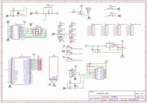
A complete and accurate schematic is the foundation of successful PCB Design.
Electronic Design Automation (EDA) software is used to create the schematic and define the electrical relationships between components.
The schematic should clearly identify:
- Resistors
- Capacitors
- Diodes
- Transistors
- Integrated circuits
- Connectors
- Power supplies
- Ground connections
- Signal paths
- Protection circuits
- Test points
Before moving to PCB layout, engineers should verify that the circuit operates according to the design requirements.
Electrical Rule Check (ERC) can help identify issues such as:
- Unconnected pins
- Incorrect pin connections
- Power conflicts
- Unexpected net connections
- Missing power inputs
- Other schematic-level rule violations
Simulation may also be appropriate for analog, power, RF, and high-speed circuits. Depending on the application, engineers may evaluate voltage levels, transient response, thermal behavior, signal integrity, impedance, or electromagnetic compatibility.
A verified schematic provides a reliable foundation for the subsequent PCB layout.
2. Design the PCB Layout
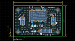
After the schematic has been verified, the electrical design is converted into a physical PCB layout.
Popular PCB design platforms include Altium Designer, KiCad, Autodesk Fusion/EAGLE, and EasyEDA. The specific software is less important than ensuring that the resulting design satisfies electrical, mechanical, and manufacturing requirements.
Component Selection and Footprints
Components should be selected based on:
- Electrical specifications
- Package availability
- Lifecycle status
- Environmental requirements
- Cost
- Assembly technology
- Supply-chain considerations
Each schematic symbol must be associated with the correct PCB footprint.
The footprint should match the component manufacturer’s recommended land pattern whenever possible.
Component Placement
Component placement should consider both electrical and manufacturing requirements.
Important considerations include:
- Functional grouping
- Signal flow
- Component orientation
- Connector accessibility
- Thermal management
- Decoupling capacitor placement
- High-speed signal paths
- Clearance
- Assembly accessibility
- Testing and rework
For example, bypass and decoupling capacitors are generally positioned close to the corresponding IC power pins to minimize parasitic inductance and current-loop area.
PCB Routing
After placement, the components are electrically connected using copper traces.
Trace width and spacing should be selected according to:
- Current requirements
- Voltage requirements
- PCB fabrication capability
- Copper thickness
- Signal integrity
- Controlled impedance requirements
- Applicable safety spacing
High-current traces may require wider traces or larger copper areas, while high-speed differential signals may require tightly controlled geometry.
Design Rule Check
After routing, a Design Rule Check (DRC) should be performed.
DRC can identify problems such as:
- Minimum clearance violations
- Trace-width violations
- Unconnected nets
- Short circuits
- Incorrect via dimensions
- Board-edge clearance problems
- Silkscreen conflicts
- Other layout-rule violations
However, passing DRC does not guarantee that a PCB is electrically or mechanically correct. A manual engineering review is still required.
3. Define the PCB Manufacturing Specifications
The next step is to determine the physical and material specifications of the PCB.
Determine the Number of Layers
The number of PCB layers depends on circuit complexity, routing density, signal integrity, power distribution, thermal requirements, and cost.
Common configurations include:
- Single-sided PCB
- Double-sided PCB
- Four-layer PCB
- Six-layer PCB
- Eight-layer PCB
- High-layer-count multilayer PCB
Multilayer designs can provide dedicated signal, power, and ground layers while reducing routing congestion.
Select the PCB Material
FR-4 is widely used for general-purpose PCBs, but specialized applications may require other materials.
Depending on operating frequency and environmental requirements, designers may consider materials such as:
- High-Tg FR-4
- Polyimide
- PTFE-based RF materials
- High-speed laminates
- Aluminum-based substrates
- Ceramic materials
Material selection can affect dielectric properties, thermal performance, mechanical stability, impedance control, and overall cost.
Select Via Structures
The design may use:
- Through vias
- Blind vias
- Buried vias
- Microvias
Through vias are generally simpler and less expensive, while blind, buried, and microvia structures can support high-density layouts.
However, advanced via technologies should only be used when necessary because they may increase fabrication complexity and cost.
Define PCB Thickness and Copper Weight
Board thickness and copper weight should be selected according to mechanical strength, current requirements, thermal performance, impedance requirements, and manufacturer capabilities.
Common copper weights include 1 oz and 2 oz, while high-current applications may require heavier copper.
The selected copper thickness also affects trace resistance, current capacity, thermal behavior, and fabrication requirements.
4. Prepare PCB Manufacturing Files
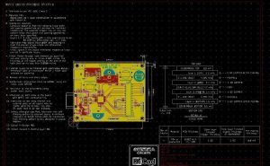
Once the layout is complete and verified, the design data must be converted into a manufacturing package.
A typical fabrication package may include:
- Gerber files
- NC drill files
- Fabrication drawing
- Stackup information
- Drill table
- Solder mask information
- Silkscreen information
- Surface-finish requirements
- Impedance requirements
- Special manufacturing notes
Gerber Files
Gerber files are commonly used to communicate PCB artwork information to fabrication equipment.
A typical Gerber package contains separate files for different PCB layers, such as:
- Top copper
- Bottom copper
- Inner copper layers
- Top solder mask
- Bottom solder mask
- Top silkscreen
- Bottom silkscreen
- Board outline
The exact file structure depends on the CAD system and manufacturer’s requirements.
Drill Files
NC drill files specify the size, position, and type of holes required for the PCB.
They may include information for:
- Through holes
- Plated holes
- Non-plated holes
- Via structures
- Mounting holes
Hole dimensions should be reviewed carefully because drilling requirements directly affect fabrication capability and cost.
Bill of Materials (BOM)
For PCB assembly, the Bill of Materials should provide complete component information.
A typical BOM may contain:
- Reference designator
- Manufacturer part number
- Component value
- Package
- Quantity
- Approved substitute
- Component description
A well-structured BOM reduces component-selection errors during assembly and purchasing.
Pick-and-Place Files
Pick-and-place files provide component location and orientation information for automated assembly equipment.
They typically contain X and Y coordinates, rotation, reference designator, and component-side information.
Assembly Drawings
Assembly drawings provide additional information about:
- Component locations
- Reference designators
- Polarity
- Orientation
- Special assembly instructions
These documents help manufacturing and inspection teams understand how the finished PCBA should be assembled.
5. Perform Design for Manufacturability (DFM) Review
Design for Manufacturability (DFM) is one of the most important steps before releasing a PCB for production.
DFM reviews whether the design can be manufactured reliably using the selected fabrication process.
Review PCB Geometry
Check:
- Minimum trace width
- Minimum spacing
- Minimum hole diameter
- Annular ring
- Copper-to-edge clearance
- Solder mask clearance
- Board thickness
- Aspect ratio
The acceptable limits depend on the manufacturer’s capabilities.
Verify Gerber Data
Before production, Gerber data should be reviewed using a suitable Gerber viewer.
The review should confirm:
- Correct layer order
- Correct board outline
- Correct copper patterns
- Correct solder mask openings
- Correct silkscreen
- Correct drill locations
- Proper alignment between layers
Check Silkscreen
Silkscreen markings should remain readable and should not overlap critical pads, component areas, or other features.
Reference designators should be positioned so they remain useful during assembly and inspection.
Review Solder Pads
Pad dimensions and spacing should be appropriate for the selected component package and assembly process.
Poor pad design can contribute to:
- Solder bridges
- Insufficient solder
- Component misalignment
- Tombstoning
- Poor solder wetting
Check Panelization Requirements
For production, the PCB may be panelized so multiple boards can be manufactured and assembled together.
Panelization should consider:
- Board spacing
- Tooling rails
- Fiducial marks
- Breakaway methods
- V-score
- Tab routing
- Component clearance from board edges
The exact panel design should be coordinated with the manufacturer.
6. Prepare for Testing and Programming

PCB testing requirements should be considered before manufacturing rather than added at the end of the project.
Designers may include appropriate test points for:
- Power rails
- Ground
- Communication interfaces
- Analog signals
- Critical control signals
Depending on the product, testing may involve:
- Flying-probe testing
- In-circuit testing (ICT)
- Functional testing
- Boundary-scan testing
- Automated test equipment
- Programming fixtures
If the PCB contains a microcontroller, memory device, FPGA, or other programmable component, programming requirements should also be considered.
Providing adequate test access can significantly simplify production testing and troubleshooting.
7. Select a PCB Manufacturer
Once the design and manufacturing documentation are complete, the next step is selecting an appropriate PCB manufacturing partner.
When evaluating a manufacturer, consider:
- PCB fabrication capabilities
- Layer-count capability
- Minimum trace width and spacing
- Minimum drill size
- Material availability
- Surface finishes
- Prototype capability
- Production capacity
- Inspection equipment
- Assembly capabilities
- Quality-management requirements
- Lead time
- Cost
Certifications and standards may also be important depending on the application. Examples include ISO 9001, UL requirements, IPC standards, or industry-specific quality systems.
Most importantly, the manufacturer should understand the technical requirements of the design before production begins.
An engineering review between the designer and manufacturer can identify potential manufacturability issues before they become production problems.
8. Build and Test a PCB Prototype
Before moving directly into mass production, building a prototype is strongly recommended for many products.
A prototype provides an opportunity to verify whether the physical PCB performs as expected.
Prototype testing may evaluate:
Electrical Performance
- Voltage levels
- Current consumption
- Signal integrity
- Communication interfaces
- Functional operation
Thermal Performance
- Component temperatures
- PCB temperature distribution
- Heat dissipation
- Thermal hotspots
Mechanical Performance
- Board dimensions
- Mounting-hole alignment
- Connector fit
- Enclosure compatibility
- Component clearance
Assembly Performance
The prototype can also reveal:
- Difficult-to-assemble components
- Incorrect footprints
- Insufficient component spacing
- Soldering problems
- Test-access problems
Issues discovered during prototyping can then be corrected before production.
Benefits of Proper PCB Manufacturing Preparation
Taking the time to properly prepare a PCB before manufacturing provides several important benefits.
Reduced Manufacturing Errors
A complete design review can identify incorrect footprints, clearance violations, missing connections, and documentation errors before fabrication.
Lower Production Costs
Early identification of design problems can reduce:
- PCB re-spins
- Scrap
- Rework
- Assembly defects
- Production delays
Correcting a design issue before manufacturing is generally more efficient than correcting it after production has started.
Improved Manufacturing Efficiency
Clear manufacturing files allow PCB fabricators and assembly teams to work with consistent and unambiguous information.
Better Product Reliability
A carefully prepared PCB is more likely to meet electrical, mechanical, thermal, and environmental requirements throughout its service life.
Easier Testing and Maintenance
Properly designed test points, clear reference designators, and accessible components can simplify production testing, troubleshooting, and future repair.
PCB Manufacturing Preparation Checklist
Before releasing a PCB for production, engineers can use the following checklist:
- Schematic completed and verified
- ERC completed
- Component specifications verified
- PCB footprints checked
- Board outline verified
- Layer stackup defined
- Component placement reviewed
- Routing completed
- Ground and power networks verified
- DRC completed
- DFM review completed
- Gerber files verified
- Drill files verified
- BOM completed
- Pick-and-place data prepared
- Assembly drawings prepared
- Test points defined
- Programming requirements confirmed
- Prototype requirements reviewed
- Manufacturing capabilities confirmed
Conclusion
Preparing a PCB for manufacturing is a structured engineering process that begins with a reliable schematic and continues through layout design, material selection, manufacturing documentation, DFM review, testing, and prototyping.
The goal is not simply to create a PCB that works electrically. A production-ready board must also be manufacturable, assemblable, testable, inspectable, and reliable.
A well-planned PCB Design process can reduce manufacturing errors, shorten development cycles, improve production yield, and control costs. At the same time, close coordination between the design team and the PCB manufacturer ensures that the final design matches actual fabrication and assembly capabilities.
For professional projects, Kingda can be considered as a PCB manufacturing and assembly partner during the design-preparation stage, helping engineering teams align PCB fabrication and assembly requirements with their production objectives.