How to Repair a PCB Pad: PCB Pad Repair, Lifted Pad & Trace Repair Guide
Printed circuit boards have become increasingly compact and sophisticated as electronic products continue to demand higher functionality, smaller dimensions, and greater reliability. A modern PCB may contain hundreds or thousands of components, with each component contributing to the overall operation of the electronic system.
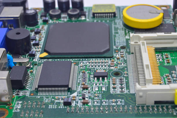
PCB pads are among the most important physical structures on a circuit board. They provide the solderable surface required to attach components and establish electrical connections between component terminals and PCB copper structures.
When a pad is lifted, cracked, partially detached, burned, corroded, or completely removed, the affected component may no longer form a reliable electrical or mechanical connection.
This makes understanding how to repair a PCB pad an important skill for PCB technicians, engineers, repair specialists, and electronics manufacturers.
PCB pad damage can result from excessive heat, mechanical stress, repeated rework, manufacturing defects, corrosion, contamination, or improper component removal. Depending on the extent of the damage, the repair may involve reflowing solder, reinforcing a lifted pad, rebuilding the pad with copper foil, repairing the connected trace, or installing a suitable jumper wire.
This guide explains how to repair a PCB pad, how to identify pad damage, why PCB pads fail, common repair techniques, and best practices for reliable PCB rework.
How to Identify a Damaged PCB Pad
Before attempting any PCB pad repair, the first step is to determine exactly what has been damaged.
A pad may appear damaged even when the underlying copper connection remains intact. Conversely, a pad may look acceptable while the associated trace, via, or internal connection has already been compromised.
A proper inspection should therefore evaluate both the visible pad and the electrical connection underneath it.
Visual Inspection
Start with a careful visual inspection under adequate lighting.
For compact or high-density PCBs, a magnifying lamp, microscope, or suitable inspection system can reveal defects that are difficult to see with the naked eye.
Look for:
- Lifted or displaced pads
- Cracked copper
- Missing copper
- Burn marks
- Discoloration
- Delamination
- Solder mask damage
- Corrosion
- Contamination
- Cracked solder joints
- Damaged traces
- Damaged vias
A partially lifted pad should be treated carefully because additional mechanical or thermal stress can cause it to detach completely.
Continuity and Resistance Testing
Electrical testing can determine whether the damaged pad remains connected to its intended net.
Use a multimeter to check continuity between the pad and an appropriate downstream test point, via, component pin, or copper feature.
However, a continuity beep alone does not prove that the pad is fully reliable. Low-resistance parallel paths and connected components can affect measurements.
For accurate troubleshooting, the PCB should normally be unpowered during continuity and resistance measurements, with capacitors discharged appropriately.
Mechanical Inspection
A pad that moves slightly under gentle inspection may indicate weakened adhesion or partial delamination.
However, technicians should avoid deliberately applying excessive force to the pad or component. Unnecessary mechanical stress can turn a repairable defect into a much larger PCB failure.
For critical or high-density boards, optical inspection and electrical testing should be combined rather than relying on mechanical testing alone.
Common Causes of PCB Pad Damage
Understanding why pads fail is essential for selecting the correct PCB pad repair method and preventing the same problem from occurring again.
Design and Manufacturing Problems
PCB design and manufacturing quality can influence pad reliability.
Important design parameters include:
- Pad dimensions
- Pad-to-pad spacing
- Annular ring
- Copper thickness
- Trace width
- Via placement
- Thermal relief design
- Solder mask clearance
- Component footprint
- Board material
Manufacturing problems such as inadequate copper adhesion, inappropriate process parameters, poor plating, excessive thermal stress, or material defects can also contribute to pad failure.
A properly designed footprint and manufacturable PCB construction can significantly reduce the risk of pad damage during assembly and rework.
Excessive Heat
Excessive heat is one of the most common causes of lifted PCB pads.
During soldering or desoldering, excessive temperature or prolonged heating can weaken the bond between the copper pad and the PCB substrate.
Repeated heating cycles can further increase the risk.
Potential thermal damage includes:
- Lifted pads
- Delamination
- Damaged solder mask
- Burned laminate
- Damaged nearby components
- Weak solder joints
- Internal layer damage
When repairing a pad, the technician should use a controlled soldering profile and avoid heating the same area for longer than necessary.
Mechanical Stress
Mechanical stress can damage PCB pads even when the electrical circuit initially appears normal.
Examples include:
- Pulling components from the board
- Twisting component leads
- Applying excessive force during desoldering
- Dropping the PCB
- Bending the board
- Pressing on components
- Improper connector removal
- Mechanical shock during transportation
Large through-hole components and connectors can be particularly demanding because mechanical forces can be transferred directly to their plated holes and surrounding copper structures.
Repeated Desoldering and Rework
Every soldering and desoldering operation introduces thermal and mechanical stress.
Repeatedly removing components from the same footprint can weaken the copper-to-laminate bond, particularly when excessive heat or mechanical force is used.
Professional rework should therefore use appropriate:
- Soldering temperatures
- Hot-air profiles
- Preheating
- Flux
- Desoldering tools
- Thermal protection
- Component removal techniques
Minimizing unnecessary rework is one of the best ways to prevent PCB pad damage.
Environmental Exposure
Moisture, corrosive chemicals, contamination, and harsh environmental conditions can gradually degrade PCB materials and exposed copper.
Potential causes include:
- High humidity
- Chemical contamination
- Corrosive atmospheres
- Improper cleaning
- Residual process chemicals
- Contaminated flux residues
- Long-term exposure to unsuitable environments
Corrosion can reduce the cross-sectional area of copper and weaken the mechanical structure of the pad.
For demanding applications, appropriate surface finishes and conformal protection may be considered according to the operating environment.
How to Repair a PCB Pad
The correct repair method depends on the severity and location of the damage.
A slightly damaged pad may require only solder rework, while a completely missing pad may require copper reconstruction and trace repair.
Method 1: Rework a Slightly Damaged Pad
If the pad is still physically attached to the PCB and the copper is largely intact, a simple solder rework may be sufficient.
A typical procedure is:
- Disconnect power from the PCB.
- Inspect the damaged area under magnification.
- Clean the area using an appropriate PCB-safe cleaning method.
- Apply a suitable amount of flux.
- Carefully reflow or rebuild the solder joint.
- Avoid excessive heat and mechanical pressure.
- Clean flux residues when appropriate.
- Inspect the repaired joint.
- Perform continuity and functional testing.
This method is appropriate only when the underlying copper structure remains mechanically sound.
Adding more solder does not repair a mechanically detached pad. If the copper itself has separated from the substrate, a structural repair is required.
Method 2: Repair a Lifted PCB Pad
A lifted pad occurs when the copper pad partially or completely separates from the PCB substrate.
If the pad remains connected to its trace and has not been completely torn away, it may sometimes be repositioned and mechanically reinforced.
A typical repair approach may involve:
- Cleaning the damaged area.
- Carefully repositioning the lifted pad.
- Verifying its electrical connection.
- Applying an appropriate PCB repair adhesive or epoxy around the pad as required.
- Allowing the adhesive to cure according to its specification.
- Re-establishing the solder connection.
- Performing electrical and mechanical inspection.
The adhesive should not contaminate the actual soldering surface or interfere with component assembly.
For high-reliability applications, the repair material and method should be selected according to the required environmental and mechanical performance.
Method 3: Rebuild a Missing PCB Pad
When a pad has been completely removed, PCB pad reconstruction may be necessary.
A replacement copper foil or suitable PCB repair pad can be cut to approximately match the original footprint.
The basic process may include:
- Remove loose or damaged material.
- Clean and prepare the repair area.
- Identify the original electrical connection.
- Prepare a replacement copper pad.
- Position the replacement pad accurately.
- Bond it to the PCB using an appropriate repair adhesive.
- Connect it electrically to the original trace or via.
- Restore the solderable surface as required.
- Inspect the repair under magnification.
- Perform electrical and functional testing.
The replacement pad should match the original footprint as closely as practical.
For fine-pitch components, the geometry of the repaired pad is particularly important because excessive size or misalignment can create solder bridging or assembly problems.
Method 4: Repair a Damaged PCB Trace
Sometimes the visible pad is only part of the problem.
If the pad has been torn away together with the connected copper trace, the trace must also be restored.
A common technique is to use a fine insulated wire or PCB repair wire as a jumper.
The general procedure is:
- Identify the original electrical net.
- Locate an accessible point where the original trace remains intact.
- Remove a small amount of solder mask if necessary.
- Prepare the copper surface.
- Solder the repair wire to the intact copper.
- Route the wire carefully.
- Secure the wire mechanically using suitable PCB-safe adhesive if required.
- Connect the other end to the repaired pad or appropriate electrical point.
- Verify continuity and isolation.
- Perform functional testing.
The repair wire should be appropriately sized for the expected current and routed so that it does not create mechanical or clearance problems.
For high-current or high-frequency circuits, a simple thin jumper wire may not adequately reproduce the electrical characteristics of the original copper structure. In such cases, a more comprehensive repair or board replacement may be preferable.
Method 5: Repair a Damaged PTH Pad
Through-hole components use plated-through holes and surrounding copper pads to establish mechanical and electrical connections.
If a PTH pad is damaged, the repair method depends on whether the plated barrel and internal connections remain intact.
A technician may need to:
- Inspect the plated hole
- Verify electrical continuity
- Rebuild the external pad
- Repair the associated trace
- Reinforce the area mechanically
- Replace the component if necessary
If the plated barrel itself has been damaged, simply adding copper to the surface may not restore the internal electrical connection.
For multilayer PCBs, this distinction is particularly important because a PTH may connect several internal copper layers.
Method 6: Repair a Via-Connected Pad
Some SMD pads are connected directly to vias.
If a pad is damaged in this configuration, the repair may involve both the pad and the via connection.
Before repairing it, determine whether the via connects to:
- Another signal layer
- A ground plane
- A power plane
- An internal trace
- Multiple PCB layers
If the via barrel or surrounding copper is damaged, the technician must restore the electrical path rather than simply replacing the visible surface pad.
Best Practices for PCB Pad Repair
Reliable PCB pad repair requires more than restoring electrical continuity. The repaired structure should also withstand soldering, component assembly, vibration, thermal cycling, and normal operating conditions as appropriate for the application.
Use Compatible Materials
Use repair materials that are compatible with the PCB substrate, soldering process, and operating environment.
Depending on the application, this may include:
- Appropriate solder
- Suitable flux
- PCB repair copper foil
- PCB-safe adhesive
- Epoxy
- Repair wire
- Protective coating
Control Soldering Temperature
Avoid excessive soldering temperatures and unnecessary heating time.
Use appropriate tip geometry, preheating, hot-air equipment, or other controlled rework methods where applicable.
Minimize Mechanical Stress
Do not pull, twist, or pry components aggressively.
When removing a damaged component, ensure the solder has been sufficiently reflowed before attempting to lift it.
Protect Nearby Components
When using hot air, protect temperature-sensitive components and materials surrounding the repair area.
Localized heating is generally preferable to unnecessarily heating a large section of the PCB.
Verify the Electrical Connection
After repairing a pad, check:
- Continuity
- Isolation from adjacent nets
- Resistance where appropriate
- Component connection
- Trace integrity
- Via connectivity
For critical circuits, functional testing should follow electrical verification.
Verify Mechanical Strength
A repaired pad should not move or lift under normal component handling and assembly conditions.
Mechanical reinforcement may be necessary when the original pad experienced significant physical damage.
Inspect Under Magnification
After completing the repair, inspect the solder joint, pad geometry, trace connection, and surrounding area under magnification.
Look for:
- Solder bridges
- Cracks
- Excess solder
- Exposed copper
- Pad movement
- Flux residues
- Damaged solder mask
- Inadequate clearance
PCB Pad Repair vs. PCB Replacement
Not every damaged PCB should be repaired.
A repair may be appropriate when:
- The damage is localized.
- The PCB is otherwise functional.
- Replacement boards are unavailable.
- The board is expensive or obsolete.
- The repair can restore the required electrical and mechanical performance.
- The repair can be properly inspected and tested.
PCB replacement may be preferable when:
- Multiple pads or traces are severely damaged.
- Internal layers are compromised.
- The PCB has extensive delamination.
- The board has suffered severe thermal damage.
- Reliability requirements cannot be demonstrated after repair.
- Repair cost approaches or exceeds replacement cost.
For safety-critical, aerospace, medical, automotive, or other high-reliability applications, repair procedures should follow the applicable product requirements, manufacturer instructions, and quality procedures.
How to Prevent PCB Pad Damage
Preventing pad failure is generally more effective than repairing it afterward.
During PCB Design
Engineers should consider:
- Appropriate pad geometry
- Adequate copper area
- Suitable annular ring
- Proper thermal relief
- Appropriate component footprints
- Mechanical reinforcement for large components
- Manufacturable trace and spacing
- Correct via placement
During PCB Assembly
Use controlled soldering and reflow profiles.
Avoid excessive manual heating, especially around small SMD pads and fine-pitch components.
During Component Removal
Use suitable desoldering equipment rather than pulling components from the PCB.
For through-hole components, ensure solder has been completely removed from the plated holes before extracting the component.
During Handling and Storage
Protect PCBs from:
- Excessive bending
- Mechanical impact
- Moisture
- Corrosive contamination
- Improper stacking
- Electrostatic discharge where applicable
Proper storage and handling can reduce both pad damage and broader PCB reliability problems.
When Professional PCB Repair Is Recommended
Simple PCB repairs can sometimes be performed by experienced technicians, but advanced damage may require professional inspection and rework equipment.
Professional assistance is recommended when the board contains:
- Fine-pitch BGA packages
- High-density HDI structures
- Internal-layer connections
- High-current paths
- High-frequency circuits
- Critical power supplies
- Safety-related functions
- Complex multilayer structures
A repair that restores continuity but changes the impedance, current capacity, thermal behavior, or mechanical strength of the original design may not be acceptable for a demanding application.
How Kingda Supports PCB Manufacturing and Repair Requirements
A reliable PCB repair strategy begins with understanding the original PCB construction and manufacturing requirements.
Kingda can support PCB projects by helping engineers evaluate manufacturing considerations such as PCB materials, copper thickness, layer structures, pad geometry, via structures, surface finish, and manufacturability.
For boards that require repair or rework, the appropriate solution depends on the actual damage. Localized pad damage may be repairable, while extensive internal-layer or structural damage may justify PCB replacement or a revised manufacturing solution.
Early technical evaluation can help determine whether repair, redesign, or replacement is the most practical approach.
Conclusion
Understanding how to repair a PCB pad is essential because pads provide both the physical soldering surface and an important part of the electrical connection between components and the PCB.
PCB pads can be damaged by excessive heat, mechanical stress, repeated rework, manufacturing defects, corrosion, and environmental exposure. The correct repair method depends on the severity of the damage and whether the associated trace, via, plated barrel, or internal layer has also been affected.
Minor damage may be addressed through controlled solder rework, while lifted or missing pads may require copper reconstruction, adhesive reinforcement, trace repair, or jumper-wire installation. PTH and via-connected pads require additional attention because the visible surface may be connected to internal PCB structures.
Most importantly, a successful PCB pad repair should restore more than electrical continuity. The repaired area should provide appropriate mechanical strength, solderability, electrical isolation, thermal performance, and reliability for its intended application.
With proper inspection, controlled rework techniques, suitable materials, and thorough post-repair testing, many localized PCB pad failures can be successfully addressed. However, when damage is extensive or the board has critical reliability requirements, professional evaluation and PCB replacement may be more appropriate than attempting a localized repair.