How to Solve EMI Problems in Multilayer PCB Design
Electromagnetic interference (EMI) is a common challenge in high-speed and multilayer PCB design. EMI can originate from power distribution networks, high-speed signal transitions, poor return paths, excessive loop areas, and inappropriate layer stack-up.
Modern EMI mitigation can involve shielding materials, EMI suppression components, filtering, simulation, and mechanical design. However, many EMI problems can be addressed much earlier through proper PCB layout and stack-up design.
This article explains how PCB Stackup Design, power and ground planes, signal return paths, and multilayer routing can work together to improve EMI Control and Signal Integrity.
1. Understand the Role of the Power Distribution Network
Placing an appropriate decoupling capacitor close to an IC power pin can reduce local power-supply impedance and provide transient current during fast switching events. However, a capacitor alone cannot provide low impedance across the entire frequency range.
Every capacitor has parasitic inductance and resistance, which limit its effectiveness at higher frequencies. Meanwhile, transient currents flowing through the power distribution network can create voltage fluctuations across inductive paths. These voltage fluctuations can contribute to common-mode EMI.
A well-designed power distribution network can significantly reduce this problem.
Power Planes as High-Frequency Energy Reservoirs
In a multilayer PCB, a closely spaced power plane and ground plane form a distributed capacitance. This plane-to-plane capacitance can supplement discrete decoupling capacitors by providing a low-inductance path for high-frequency transient currents.
The closer the power and ground planes are, the greater the distributed capacitance and the lower the inductance of the current path.
However, the actual effectiveness depends on:
- Dielectric thickness
- Dielectric constant
- Plane geometry
- Operating frequency
- Current distribution
- PCB material
- Component placement
- Via inductance
Therefore, plane spacing should be selected according to the complete electrical and manufacturing requirements rather than using a single universal value.
Keep Power Connections Short
The connection between an IC power pin and its decoupling network should be as short and low-inductance as practical.
For high-speed devices, even a small amount of parasitic inductance can produce significant voltage transients. Decoupling capacitors should therefore be placed close to the relevant power pins, with short traces and appropriately designed vias.
A well-engineered Multilayer PCB should combine local decoupling with low-inductance power and ground planes rather than relying on either approach alone.
2. Use PCB Layer Stack-Up for EMI Shielding
A good multilayer stack-up places high-speed signal layers close to continuous reference planes.
For most high-speed designs, a signal layer should have an adjacent ground or power reference plane. This arrangement provides a controlled return path and reduces the area of the signal-current loop.
For the power distribution system, placing power and ground planes close together can also reduce plane impedance and improve high-frequency current distribution.
This is one of the fundamental principles of EMI Shielding in PCB design.
The goal is not simply to increase the number of PCB layers. Instead, each layer should have a clearly defined electrical function.
A typical high-performance stack-up may include:
- Signal layers
- Ground planes
- Power planes
- Additional signal layers
- Dedicated reference planes
The exact arrangement should be determined by routing density, impedance requirements, power distribution, component placement, and manufacturing constraints.
3. Four-Layer PCB Stack-Up for EMI Control
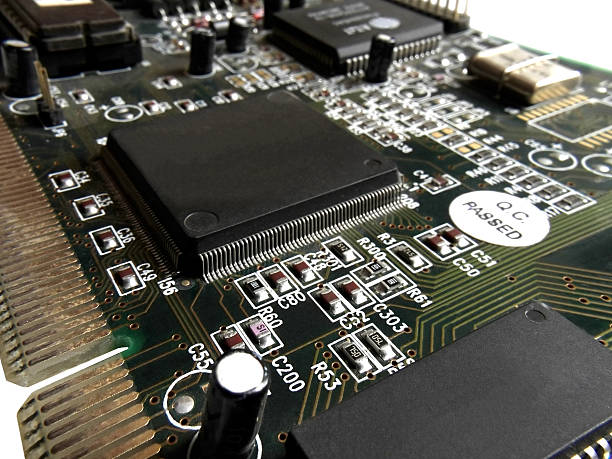
A conventional four-layer PCB often uses two external signal layers with internal power and ground planes. This structure can work well for many applications, but the distance between the power and ground planes may be relatively large depending on the finished board thickness and dielectric construction.
When EMI performance is important, alternative four-layer stack-ups can be considered.
Option 1: Ground–Signal/Power–Signal/Power–Ground
One approach is to place ground on both external layers while using the inner layers for signals and power distribution.
Power can be routed using wide conductors or copper regions on the signal layers. This can reduce power-path impedance while providing close reference planes for signal routing.
From an EMI perspective, this structure can provide strong shielding when the layout and copper distribution are carefully controlled.
However, it requires sufficient board area and component-placement flexibility.
Option 2: Power/Ground–Signal–Signal–Ground/Power
Another approach places power and ground on the outer layers and uses the inner layers primarily for signal routing.
This can improve the reference environment compared with some conventional four-layer structures, but the electrical performance depends heavily on dielectric thickness, copper distribution, routing geometry, and how effectively the outer planes are connected.
For either approach, copper areas should not be treated as isolated islands. Where practical, ground regions should be connected with sufficient stitching vias and maintained as continuous reference structures.
For impedance-controlled designs, traces should be routed over a continuous reference plane rather than across plane gaps or isolated copper regions.
4. Six-Layer PCB Stack-Up for EMI and Signal Integrity
When component density and routing requirements exceed what a four-layer board can accommodate, a six-layer PCB often provides a better balance between routing capacity, power distribution, and EMI performance.
However, not every six-layer stack-up provides the same electrical performance.
Stack-Up Example 1: Signal–Power–Signal–Signal–Ground–Signal
Placing power and ground relatively far apart can provide useful routing flexibility and may simplify certain impedance-control requirements.
However, the power distribution network may have higher impedance than a closely coupled power-ground pair. This can reduce the effectiveness of the planes as a high-frequency current path and potentially increase common-mode noise.
Therefore, this structure should be evaluated based on the actual power-distribution and EMI requirements.
Stack-Up Example 2: Signal–Signal–Power–Ground–Signal–Signal
Placing power and ground next to each other creates a tightly coupled plane pair, which can reduce plane impedance and improve high-frequency power distribution.
The disadvantage is that the outer signal layers may have less direct electromagnetic shielding from adjacent reference planes depending on the dielectric construction.
If the external signal traces are short and carry relatively low-frequency content, the structure can still perform well.
Grounded copper areas and stitching vias can also be used to improve shielding around sensitive regions, provided they are designed as part of a controlled return-current structure.
A Practical High-Performance Six-Layer Structure
A commonly useful high-performance arrangement is:
Signal – Ground – Signal – Power – Ground – Signal
This provides close reference planes for multiple signal layers while maintaining a dedicated power-ground pair.
The structure can support good signal integrity and EMI performance, but the stack-up must remain mechanically and electrically balanced.
An apparently good electrical stack-up can still create manufacturing problems if copper distribution and dielectric construction are highly asymmetric.
Therefore, stack-up development should consider both electrical performance and PCB fabrication requirements.
5. Ten-Layer PCB Design for High-Speed Signals
As PCB layer count increases, dielectric layers can be engineered to create tightly coupled signal-reference structures.
A ten-layer board can provide significantly more routing capacity while allowing engineers to separate signal, power, and ground functions.
One possible high-performance structure is:
Signal – Ground – Signal – Signal – Power – Ground – Signal – Signal – Ground – Signal
The important principle is not the exact sequence itself, but the relationship between each signal layer and its reference plane.
A signal should ideally remain close to its intended return path.
Maintain a Short Signal Return Path
Consider a high-speed signal routed on Layer 1 with its return current flowing primarily on the adjacent Layer 2 ground plane.
If the signal changes layers through a via and moves to another layer, the return current must also transition appropriately.
If the return path is interrupted, the current may be forced to travel around a plane split or search for another grounding path. This increases loop area and parasitic inductance and can increase both EMI and signal-integrity problems.
This is one of the most important principles of high-speed Signal Integrity design.
Use Ground Vias Near Signal Vias
When a high-speed signal changes routing layers, placing a nearby ground stitching via can provide a lower-inductance transition for the return current.
This is particularly important when a signal transitions between layers with different reference planes.
The ground via provides a nearby path for the return current to transition between reference structures, helping maintain a compact current loop.
For high-speed interfaces, via placement should therefore be considered from both the signal path and return-path perspectives.
6. Routing Direction and Layer Pairing
In multilayer high-speed designs, routing directions can be coordinated between different signal layers.
For example:
- Layer 1: X-direction
- Layer 3: Y-direction
- Layer 4: X-direction
- Layer 7: Y-direction
- Layer 8: X-direction
- Layer 10: Y-direction
The exact routing direction is application-dependent, but alternating routing directions can reduce unnecessary parallel coupling between adjacent layers.
More importantly, each signal layer should maintain a well-defined reference plane.
When a signal changes routing direction through a via, the return-current path must be considered at the same time.
This prevents the common mistake of optimizing only the forward signal path while ignoring the return path.
7. Multilayer PCB Design with Multiple Power Rails
Some systems require multiple power rails or multiple power planes.
When two planes carry current from the same voltage source, engineers should consider whether the planes have similar impedance and comparable current paths.
If the power-plane structures have significantly different impedance, current sharing may become uneven.
Uneven current distribution can increase transient voltage and potentially worsen EMI.
For high-current power distribution, a practical strategy is to create well-defined power-ground pairs and optimize their geometry so that current paths remain short and predictable.
When multiple voltage rails are present, each power domain should also be carefully separated according to:
- Voltage level
- Current requirement
- Noise sensitivity
- Switching frequency
- Grounding strategy
- Return-current path
- Layer-to-layer coupling
Power-plane placement should also consider PCB manufacturing balance.
8. PCB Manufacturing Must Be Considered During Stack-Up Design
Electrical optimization cannot be separated from manufacturability.
A theoretically excellent stack-up may create problems if copper distribution, dielectric thickness, lamination construction, or overall board thickness falls outside practical manufacturing capabilities.
For high-layer-count boards, layer registration, dielectric thickness, resin distribution, copper balance, and lamination control become increasingly important.
A professional PCB Manufacturing process should therefore evaluate the proposed stack-up before fabrication.
This is particularly important for:
- High-speed PCBs
- High-density multilayer PCBs
- High-layer-count PCBs
- Controlled-impedance PCBs
- HDI PCBs
- High-frequency PCBs
GOPCBA supports multilayer, HDI, high-speed, high-frequency, controlled-impedance, rigid-flex, and other advanced PCB structures.
9. Common EMI Control Mistakes in Multilayer PCB Design
Several layout problems can undermine an otherwise good stack-up.
Routing Across Plane Splits
A high-speed signal should not cross a split in its reference plane without carefully analyzing the return-current path.
The return current may be forced to detour around the split, increasing loop area and radiation.
Excessive Via Distance
If a signal changes layers but its return current has no nearby transition path, the return loop can become large.
Ground stitching vias should therefore be placed strategically around high-speed transitions.
Discontinuous Ground Planes
A fragmented ground plane can create unexpected return-current paths and increase EMI.
For sensitive high-speed interfaces, continuous reference planes are generally preferred.
Excessive Parallel Routing
Long parallel traces can increase crosstalk and electromagnetic coupling.
Where possible, routing layers should be arranged to minimize long parallel runs between sensitive signals.
10. How to Improve EMI Performance Before PCB Fabrication
EMI problems are much easier and less expensive to address during the design stage than after prototype fabrication.
Before manufacturing, engineers should verify:
- Whether every high-speed signal has a clear reference plane.
- Whether signal return paths are continuous.
- Whether power and ground planes are appropriately coupled.
- Whether high-speed traces cross plane splits.
- Whether signal vias have suitable return-current paths.
- Whether ground stitching vias are required.
- Whether copper distribution is sufficiently balanced.
- Whether the proposed stack-up meets impedance requirements.
- Whether dielectric thickness and material are suitable for the target frequency.
- Whether the stack-up is compatible with the manufacturer’s fabrication process.
For complex multilayer designs, engineering review and DFM analysis can identify potential stack-up, spacing, registration, and manufacturing problems before production. GOPCBA provides PCB design and layout support for multilayer, high-speed, HDI, impedance-controlled, and other advanced PCB designs.
11. Why PCB Stack-Up Is Critical to EMI Control
The number of PCB layers alone does not determine EMI performance.
A well-designed four-layer PCB can outperform a poorly designed eight-layer PCB if the four-layer board provides better reference-plane continuity, shorter return paths, lower loop inductance, and better power distribution.
The key factors include:
- Reference-plane continuity
- Signal-to-plane spacing
- Power-ground coupling
- Return-current path
- Loop area
- Via transitions
- Impedance control
- Copper distribution
- Material selection
- Manufacturing tolerances
For high-speed systems, PCB Stackup Design should therefore be treated as part of the electrical design rather than simply a mechanical arrangement of copper layers.
12. Final Design Principles for EMI Reduction
Effective EMI Control in multilayer PCB design is based on controlling current paths.
The most important principles are:
- Keep high-speed signals close to continuous reference planes.
- Minimize signal-loop area.
- Keep power and ground planes closely coupled where appropriate.
- Place decoupling capacitors close to IC power pins.
- Provide low-inductance return paths.
- Use ground vias near critical signal transitions.
- Avoid routing across reference-plane gaps.
- Reduce unnecessarily long parallel signal runs.
- Balance copper distribution across the PCB stack-up.
- Verify impedance and dielectric construction before fabrication.
- Evaluate the stack-up together with the manufacturer’s process capability.
As IC edge rates continue to increase, PCB designs become increasingly sensitive to parasitic inductance, return-path discontinuities, and electromagnetic coupling. Proper stack-up engineering therefore plays an essential role in achieving both low EMI and reliable signal transmission.
The objective of a high-performance Multilayer PCB is not simply to add more layers, but to create a controlled electrical environment in which signal currents, return currents, power currents, and reference planes work together.
By combining proper PCB Stackup Design, continuous reference planes, controlled impedance, low-inductance power distribution, and carefully managed return paths, engineers can significantly improve EMI Shielding, reduce unwanted radiation, and maintain reliable Signal Integrity.