In-Circuit Test Fixture Design: Probes, Access and Maintenance
A bed of nails fixture connects every net on a board to the tester through a spring probe. The design of that fixture determines whether the test is reliable, maintainable and worth the cost of building it.
What the Fixture Must Do
The fixture must hold the board in a fixed position, press every probe against its target with a controlled force, and connect those probes to the tester without adding resistance or noise that affects the measurement.
It must also be robust enough to survive thousands of board loadings without a probe losing contact, and it must be serviceable, because a single faulty probe stops the line until it is replaced.
The mechanical design and the electrical design are therefore the same problem, and a fixture that solves one at the expense of the other will fail in production.
Choosing the Probe Points
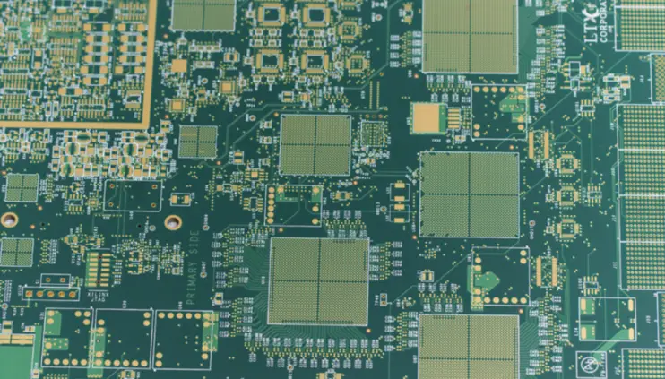
A test point must be accessible from the side where the fixture probes, must be large enough for the probe tip, and must not be shared with a component. Our flying probe notes describe the access requirements in a related context.
Points on the solder side are the norm for a single sided fixture, which means that components on that side must not obstruct the probe. A board with parts on both sides needs either two fixtures or a fixture that probes only where the geometry permits.
Vias used as test points must be capped or tented consistently, because an open via makes contact unreliable and can wick solder away from a joint. A dedicated test pad with a defined size is the more reliable choice.
Probe Force and Board Support
Each spring probe generates a force of a few newtons, and a board with a thousand probes therefore experiences a load of a few thousand newtons. The board must be supported across its whole area, not only under the test points that the designer had in mind.
Support posts, or a support plate machined to the board’s contour, spread the load and prevent flexing. Flexing changes the contact force at individual points and can crack a solder joint or a component.
Where the board carries tall components on the probed side, the support must be shaped around them, which is more expensive than a flat plate and is the price of probing that side.
Fixture Wiring and Signal Integrity
The wires from the probes to the tester are part of the measurement circuit. They add resistance, which matters for a resistance measurement, and they add inductance, which matters for a fast signal.
Wire length should be kept as short and as uniform as possible, and the wires carrying sensitive measurements should be routed away from those carrying switching signals. A fixture that works on the bench can fail on the line because of a cable run that was changed during installation.
Where the test measures a low resistance or a small voltage, the fixture is a four terminal system and the probe contact resistance must be excluded from the measurement. The tester’s connection scheme determines whether that is done automatically or must be provided by additional probes.
Vacuum, Mechanical and Pneumatic Actuation
A vacuum fixture pulls the board down onto a gasket and uses the pressure difference to generate the contact force. It requires the board to be flat, and it produces a uniform force across the board.
A mechanical fixture presses the board down with a lever or a press, which allows higher forces and does not require a vacuum source. It relies on the mechanical alignment of the press to distribute the force evenly.
A pneumatic fixture combines the two and allows the force to be programmed. Whatever the method, the force must be repeatable, because an inconsistent force produces inconsistent contact resistance.
Maintenance and Probing Reliability
Spring probes wear and their contact resistance rises with use. The fixture should record the number of loadings, and the probes should be replaced on a schedule or when the measured contact resistance drifts.
Debris on the probe tips, flux residue on the test pads and solder paste on the board all reduce contact quality. A cleaning routine for the board and for the fixture is part of the test process rather than an optional extra.
Where a probe point is used for thousands of boards, the pad itself wears. Our coupon notes describe how test structures are placed so that wear is measurable rather than fatal.
Program Development and Coverage
The test program defines what each measurement is compared against and what happens when it fails. Developing the program alongside the fixture is cheaper than adapting a program written for another product.
Coverage is the proportion of the nets and components that the fixture can actually verify. A fixture with good coverage catches assembly defects that functional test would miss, which is the reason to build it.
Our AOI notes describe the defects that optical inspection covers, which is the complementary set to what the fixture tests.
Cost and the Decision to Build
A fixture is a fixed cost that is justified by the volume and by the value of the defects it catches. For a low volume product, a flying probe test may be more economical because it needs no fixture at all.
For a high volume product, the fixture pays for itself quickly, and the engineering effort in designing the test points properly is recovered in reduced false failures.
Our solder defects notes describe the failure modes that the fixture is expected to catch, which is the basis for the coverage decision.
Process Control and Verification
On a design of this kind, probe is the item that decides how the rest of the board is arranged. Keeping a sample from the panel turns a dispute into a measurement, because the same coupon can be re-examined by both parties without rebuilding the batch. Reviewing the design before the data is released is cheaper than correcting it after the panel is in the tank, because every step downstream inherits the decision made at the front end.
Documenting the assumption is part of the design work, and a short note on the drawing prevents a question that would otherwise arrive a day later and cost a day of schedule.
Process Control and Verification
On a design of this kind, probe is the item that decides how the rest of the board is arranged. Keeping a sample from the panel turns a dispute into a measurement, because the same coupon can be re-examined by both parties without rebuilding the batch. Reviewing the design before the data is released is cheaper than correcting it after the panel is in the tank, because every step downstream inherits the decision made at the front end.
FAQ
How big should a test pad be? Large enough for the probe tip plus the placement tolerance of both the fixture and the board, which usually means a pad comparable to a via land rather than a fine trace end.
Can a via without a pad be used as a test point? It can, and it is less reliable. A tented via cannot be probed at all.
What does gopcb provide for in-circuit test? We provide test point placement review against the fixture type, pad sizing for the probe, support plans for the panel and the assembly, and the records that tie a test failure to the process step that caused it. Where the access is insufficient, we propose design changes rather than building a fixture that cannot reach.